Introduction: The Disappearing Act of Manufacturing and the Rise of Power
If the semiconductor industry were likened to a modern-day gold rush, wafer foundries would undoubtedly be the manufacturers of the most advanced digging tools, and IC design companies the adventurers with maps, searching for gold mines. However, between these two, there exists a group that is even more discreet, more profitable, and absolutely indispensable.
They don't get their hands dirty, don't break a sweat, don't own vast factory equipment, and don't even handle the final chip products. Yet, everyone who wishes to enter the mine must first pay them a "toll fee."
This is Silicon Intellectual Property (IP).
In the past, semiconductors were a race centered on "manufacturing"; but today, as Moore's Law gradually approaches its physical limits, this race has shifted towards "design efficiency" and "architectural innovation." To understand why global IP giants command higher price-to-earnings ratios than wafer foundries, we must delve into this domain, often called the "semiconductor armory," and deconstruct how it has become the most formidable moat in the modern technology industry.
Chapter One: The Curse of Moore's Law and "Design Collapse"
To understand IP, it's not enough to simply state its utility; one must first grasp the pain the industry once endured. The birth of the IP industry, in fact, originated from a "design productivity crisis."
In the early days of semiconductor development (the IDM era), giants like Intel or TI handled everything from transistor design and circuit planning to wafer manufacturing in-house. It was an era of self-sufficiency. However, as process technology advanced from micrometers to nanometers, the number of transistors inside chips surged from tens of thousands to tens of billions. This brought about a severe side effect: "design complexity" increased exponentially, while human engineers' productivity could only grow linearly.
This phenomenon is known in the industry as the "Design Productivity Gap."
Imagine, if you were to design an AI chip using advanced process technology, the cost of masks alone could amount to hundreds of millions of dollars. This implies an extremely high cost of "trial and error"; you would barely get a second chance. If a tiny memory control circuit were poorly designed, leading to signal delays, the entire chip could become scrap silicon, and an investment of hundreds of millions would instantly turn to ashes.
In this high-pressure environment, IC design companies face a dilemma:
- Time-to-Market Pressure: Consumer electronic products have lifecycles measured in months. If a chip is launched two months late, market share can be completely captured by competitors.
- Resource Limitations: Even with the world's smartest engineering team, it would be impossible for them to "hand-craft" every USB interface or every WiFi module circuit from scratch. That would be an extreme waste of top-tier talent.
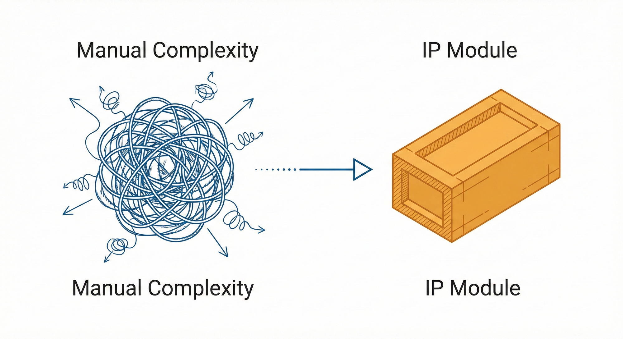
Consequently, the industry evolved a "salvation through specialization." Circuit design departments, which were originally internal to major companies, began to separate those "non-core, standardized, and highly repetitive" circuit modules, turning them into marketable products.
This is the essence of IP: it "encapsulates" engineers' intelligence into standardized products, allowing newcomers to directly purchase others' intellectual output, much like buying Lego bricks. This is not just about saving money; it is the sole solution for sustaining Moore's Law under physical limits.
Chapter Two: Deconstructing "Passive Income" — A Nearly Perfect Business Model
The reason why capital markets flock to the IP industry, assigning it extremely high valuations, is not blind speculation. It is because the IP industry possesses a financial structure unparalleled by other hardware manufacturing industries.
Traditional manufacturing earns its money the hard way, with high revenue but low gross margins. While wafer foundries have high gross margins, they must invest astronomical capital expenditures (CapEx) annually to build factories and purchase equipment, leading to immense depreciation pressure. In contrast, the IP industry operates with "zero inventory, zero factories, and extremely high gross margins."
A typical IP company usually has gross margins between 80% and 100%. Their only costs are "human intellect" (salaries for R&D engineers) and expensive EDA software licensing fees. Once an IP is developed, it can be replicated and sold to customers worldwide an infinite number of times, with marginal costs approaching zero.
Even more appealing is its "compounding" fee mechanism, a dual-engine system that ensures a continuous flow of cash:
1. Upfront: License Fee — The Entry Ticket
When a client initiates a project and decides to adopt a certain company's architecture (e.g., a USB 4.0 controller), this fee must be paid upfront. This is a one-time "toll fee," typically used to support the IP company's current operations and R&D costs. This ensures that the IP company generates revenue even before the product is launched.
2. Later Stage: Royalty — The Right to Collect Tax
This is the main course, and also Warren Buffett's favorite "toll bridge" model. After the client's chip design is complete, mass-produced by a wafer foundry, and sold into the market, the IP company collects a percentage (typically 1% to 3%) based on the "number of chips sold" or the "wafer price."
The power of this mechanism lies in the "long tail effect" and "accumulative nature."
Imagine an IP company that licensed a power management IP to a client five years ago. Today, five years later, that chip is still widely used in hundreds of millions of home appliances or automobiles. The IP company no longer needs to invest any human resources, yet it receives the "fruits" planted five years ago every month.
As time progresses, a mature IP company accumulates thousands of older projects that are still in mass production. The stable cash flow generated by these older projects, stacked upon the license fees from new projects, forms a formidable profit flywheel. This is why IP stocks tend to be relatively resilient during economic downturns, as their revenue streams are the sum of accumulations over the past decade, rather than solely dependent on current economic conditions.
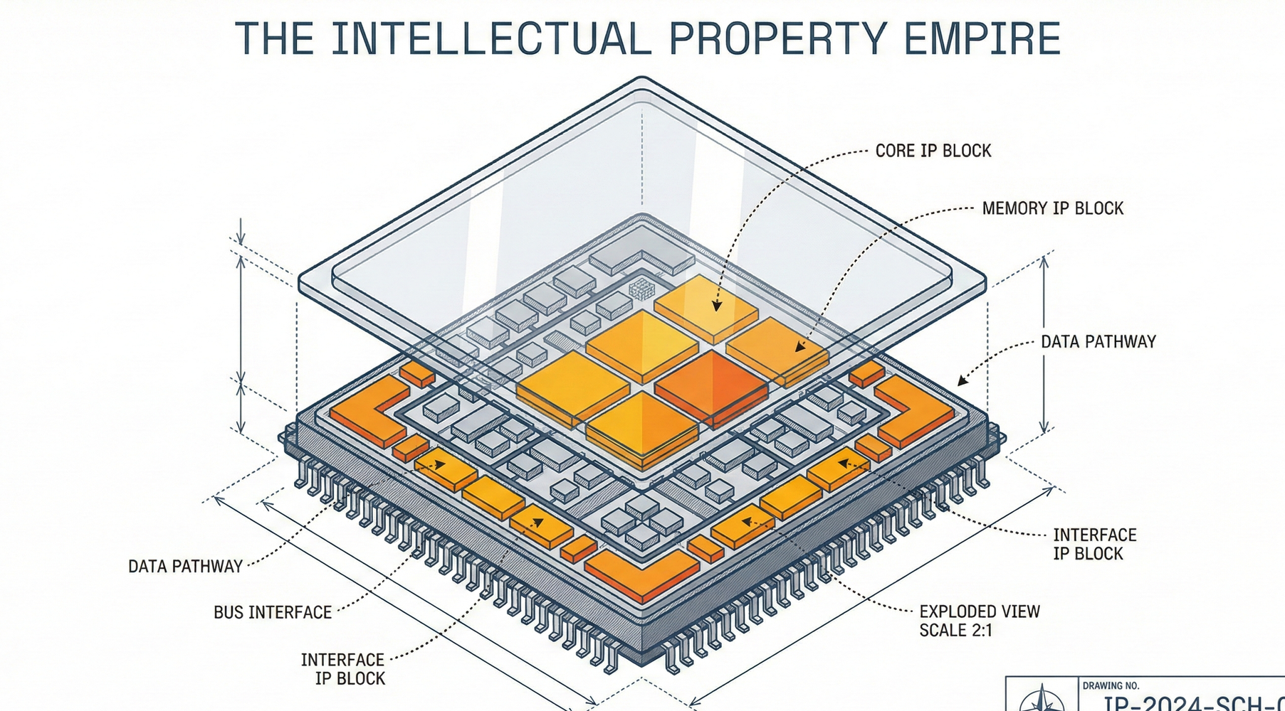
Chapter Three: Chip Anatomy — Three Destiny-Defining Building Blocks
Not all IP is created equal. In the skyscraper of a chip, different IPs occupy distinct strategic positions, which also determine the depth of a vendor's moat. We can categorize them into three main types:
1. The Crown Jewel: Processor IP
This is the soul and brain of the chip, and also the area with the highest technical barriers and deepest ecosystem lock-in.
- Function: The control center responsible for directing computations and logical decisions (e.g., CPU, GPU, NPU).
- Strategic Position: Extremely monopolistic. Processor IP is not merely circuit design; it is an "Instruction Set Architecture (ISA)." Once software developers become accustomed to a certain architecture (e.g., ARM architecture), the cost of switching architectures is unimaginably high, as all software would need to be rewritten. This is why ARM has achieved a near-monopolistic position in the mobile device sector—it controls not just the hardware, but the entire software ecosystem.
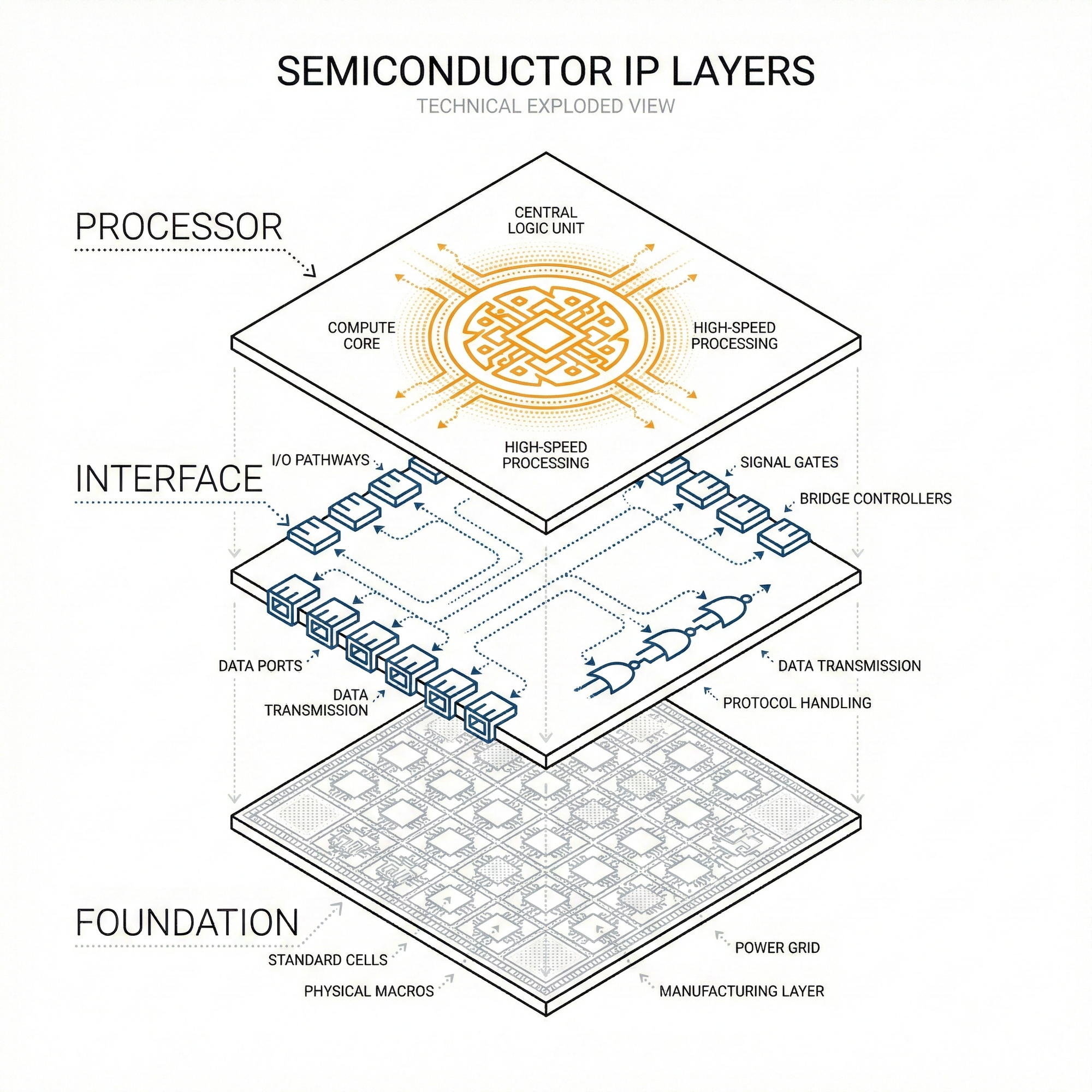
2. Bridges to the World: Interface IP
With the explosion of big data and AI computing demands, while internal chip processing is fast, data transmission often gets "stuck at the gate," leading to the golden age of high-speed interface IP.
- Function: Responsible for data throughput between the chip's internal components and external systems.
- Technical Core: SerDes (Serializer/Deserializer). This is the key technology that enables high-speed data entry and exit from the chip.
- Market Drivers: A key characteristic of this type of IP is its "high standardization." Whether it's USB, PCIe (for connecting graphics cards), DDR (for connecting memory), or HDMI, these standards adhere to strict international specifications. IC design companies simply don't need to spend time developing these standardized products themselves; the most reliable strategy is to purchase off-the-shelf solutions from major vendors like Synopsys or Cadence. This type of IP is an "essential demand"; as long as a chip needs to connect to a network or transmit data, it is indispensable.
3. Foundational Infrastructure: Physical / Foundation IP
This type of IP may seem the least remarkable, yet it is the most deeply tied to wafer foundries.
- Function: These are like the "cells" and "bricks" of a chip, such as standard cell libraries, memory compilers, or I/O components.
- Moat: The moat here lies in "validation." Whenever a wafer foundry develops a new process (e.g., advancing from 5nm to 3nm), it requires IP partners to cooperate in developing the corresponding basic component libraries. Design companies only dare to use IP that has been validated by the foundry. This "process-bound" characteristic creates a symbiotic relationship between physical IP suppliers and foundries, establishing extremely high barriers to entry.
Chapter Four: The Power Landscape of Global IP Giants
In the global IP landscape, although there are many competitors, power is highly concentrated in the hands of a few European and American giants. Understanding their positions is crucial to grasping the industry's rules of the game.
- ARM: The Absolute Dominator of Mobile Devices ARM, based in the UK, is synonymous with processor IP. Over 95% of smartphones globally use ARM's architecture. Its business model extends beyond selling IP; it manages a vast ecosystem. From Apple to Qualcomm, MediaTek to Samsung, all are ARM clients. Every update to its instruction set sends ripples throughout the global tech industry.
- Synopsys & Cadence: EDA Duopoly's Dimensionality Reduction Attack These two US companies originally specialized in EDA (Electronic Design Automation software), essentially selling "drawing tools." However, they later realized that since clients were using their software to design, they might as well sell the completed designs (IP) too. Leveraging their software monopoly, they have achieved a dominant position in "interface IP" (such as USB, DDR). Clients often find it convenient to purchase software and IP together, creating a powerful bundling effect.
Chapter Five: The Battlefield of the Future — Chiplet, RISC-V, and AI
The semiconductor IP industry is not static; three major technological trends are reshaping the market's boundaries and opening opportunities for new entrants to challenge the giants.
1. The Chiplet Revolution: The Physicalization of IP
As Moore's Law slows down, cramming all functions into a single large chip (SoC) becomes expensive, difficult to manufacture, and yields are low. The future trend is "divide and conquer" — making CPU, GPU, memory, and other functions on separate smaller chips using the most suitable processes, then assembling them like a puzzle with advanced packaging technologies. This is a massive transformation for the IP industry. In the past, IP was a soft "design blueprint"; in the Chiplet era, IP might directly be sold as individual physical "chiplets." This also drives explosive demand for Die-to-Die transmission interface standards (such as UCIe).
2. The Rise of RISC-V: Breaking Monopoly with Open Architecture
For a long time, x86 (Intel) and ARM architectures monopolized the market. However, with increasingly expensive licensing fees and geopolitical concerns (fear of US sanctions), the open-source RISC-V architecture is becoming a new industry favorite. RISC-V is like Linux for chips; it allows anyone to use its instruction set for free. This gives emerging IP companies a huge opportunity to develop customized cores based on RISC-V, without being constrained by ARM's licensing terms. This is sparking a revolution in the Internet of Things (IoT) and automotive electronics fields.
3. The AI Customization Frenzy
AI algorithms are evolving rapidly. While general-purpose GPUs are powerful, they can be too expensive or power-hungry for specific applications. Consequently, tech giants like Google, Amazon, and Tesla are increasingly developing their own chips. This has led to a surge in demand for IP for "customized computing units." These giants require Neural Processing Unit (NPU) IP that can be flexibly adjusted and optimized for specific AI models, opening up a massive blue ocean for IP vendors specializing in AI computing.
Conclusion: Collecting Tolls on the Shoulders of Giants
Looking back at the semiconductor industry chain, equipment manufacturers sell tools, wafer foundries sell capacity, and IP companies sell the "leverage of knowledge."
This is an industry that places extreme importance on "trust" and "ecosystems." A new competitor might quickly design a chip, but it would be incredibly difficult to build a library of thousands of validated IPs in a short period, let alone earn the trust of global developers. This high barrier ensures supernormal profits for existing players.
For investors or industry observers, focusing on the IP industry is not just about technology; it's about observing the "power structure" of the semiconductor industry. Who defines the future transmission standards? Who controls the next-generation computing architectures? These are the entities that will quietly reap the richest profits behind the humming machines of TSMC.
In a world increasingly rich in silicon content, IP companies are not just arms dealers; they are the ones who set the rules of engagement. And this battle for rules is just entering its most exciting chapter.
In-depth Research · Quantitative Perspective
Want more quantitative research insights on semiconductors?
【Insight Subscription Plan】Break Free from Retail Investor Mentality: Build Your Alpha Trading System with "Quantitative Chips" and "Consensus Data"EDGE Semiconductor Research
📍 Series Map — Navigate the Complete EDGE Semiconductor Research →


