1-1-2 GPU vs. ASIC: The 'Soul War' for AI and the Struggle with Physical Limits
This is not just a market share battle, but a physical limits struggle between general-purpose and specialized computing. Analyzing NVIDIA GPU's SIMD vs. Google TPU's systolic array, ASICs gain TCO advantages by eliminating "dark silicon" and breaking the "memory wall." As PyTorch erodes CUDA's m...
1-1-2 GPU vs. ASIC: The 'Soul War' for AI and the Struggle with Physical Limits
Preface: Silicon Valley's Rebellion
In 2024, as NVIDIA's market cap surpassed three trillion US dollars and Jensen Huang was hailed as the Napoleon of the AI era, a silent rebellion was brewing beneath the surface of Silicon Valley.
This rebellion was not initiated by rival AMD, but by NVIDIA's largest customers—Google, Microsoft, Amazon (AWS), and Meta. While smiling and signing multi-billion dollar H100 orders, they were simultaneously toiling day and night in their secret labs, developing weapons capable of "killing" the GPU.
In the eyes of Wall Street, this is a commercial negotiation to gain control over the supply chain; but for top chip architects, it is a philosophical war about the nature of computation. It is the confrontation between "Von Neumann architecture" and "Dataflow architecture," and a desperate struggle between "general-purpose computing power" and "specialized computing power" to squeeze out every last drop of physical performance in an era where Moore's Law is considered dead.
To understand the landscape of AI chips after 2026, we must, like surgeons, cut open the packaging and look directly into the soul of the chip.
Chapter One: The Curse of Architecture — The Zero-Sum Game of Generality and Efficiency
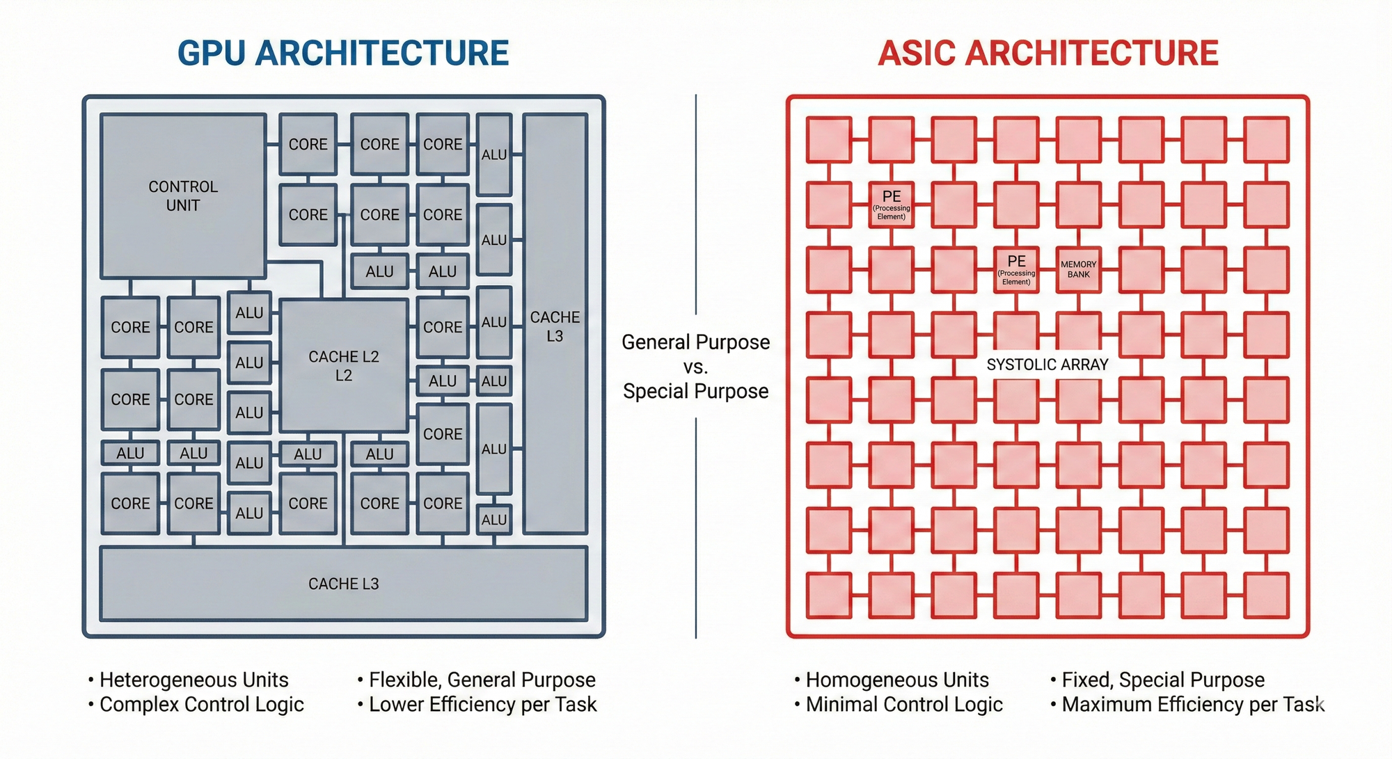
If we compare chips to vehicles, a GPU is an "all-terrain vehicle" that can travel on any terrain, while an ASIC is a "maglev train" designed for a specific track.
1. NVIDIA GPU: The Brutal Aesthetics of Parallel Computing (SIMD)
The GPU (Graphics Processing Unit) was born to process pixels on a screen. Pixel processing has a specific characteristic: the computational logic for each pixel is the same, only the data differs. This laid the foundation for the GPU's core genetic code: SIMD (Single Instruction, Multiple Data).
Inside an NVIDIA H100 chip, there are tens of thousands of CUDA Cores. They are like a disciplined army: when the commander (control unit) issues a "forward" command, tens of thousands of soldiers (processing units) simultaneously step forward with their left foot.
【The Fatal Price: Dark Silicon】 However, this architecture pays a huge price to maintain "generality." To enable the GPU to run AI Transformer models, render ray-tracing effects in "Black Myth: Wukong," and even help scientists simulate protein folding, NVIDIA must reserve a large number of "Control Logic," "Branch Prediction," and "Cache Management" circuits on the chip.
In pure AI matrix operations, these circuits are often not utilized, yet they still occupy valuable wafer area and continuously consume power. This is known in the industry as "Dark Silicon" or "Redundancy." You might spend $30,000 on a GPU, but perhaps only 40% of its transistors are working for your AI model, with the others "on standby" or "providing logistical support."
2. Google TPU (ASIC): The Ultimate Efficiency of Systolic Arrays
Google recognized this problem as early as 2015. While the world was running deep learning on GPUs, Google realized that providing speech recognition services on billions of mobile phones using GPUs would bankrupt the company.
Thus, the TPU, a flagship example of an ASIC (Application-Specific Integrated Circuit), was born. It adopted a retro yet extremely efficient architecture: Systolic Array.
【Operating Principle: The Heartbeat of Data】 Imagine a heart (Systolic means contraction). In the TPU's architecture, data is not static; it "flows" like blood. When data enters the chip, it flows through an array composed of thousands of multipliers. After data completes its operation in the first unit, it is directly passed to its neighbor for the next step, much like an assembly line in a factory or a bucket brigade during a fire.
【Advantages of ASIC】 This architecture eliminates 90% of the control units and cache within a GPU. It does not require complex instruction scheduling because the data flow path is hardcoded.
Area Efficiency: For the same 100mm² chip area, an ASIC can fit 3 to 5 times more arithmetic logic units (ALUs) than a GPU.
Performance per Watt: Due to the absence of power consumption from redundant circuits, an ASIC's energy efficiency for specific tasks is often more than 10 times that of a GPU.
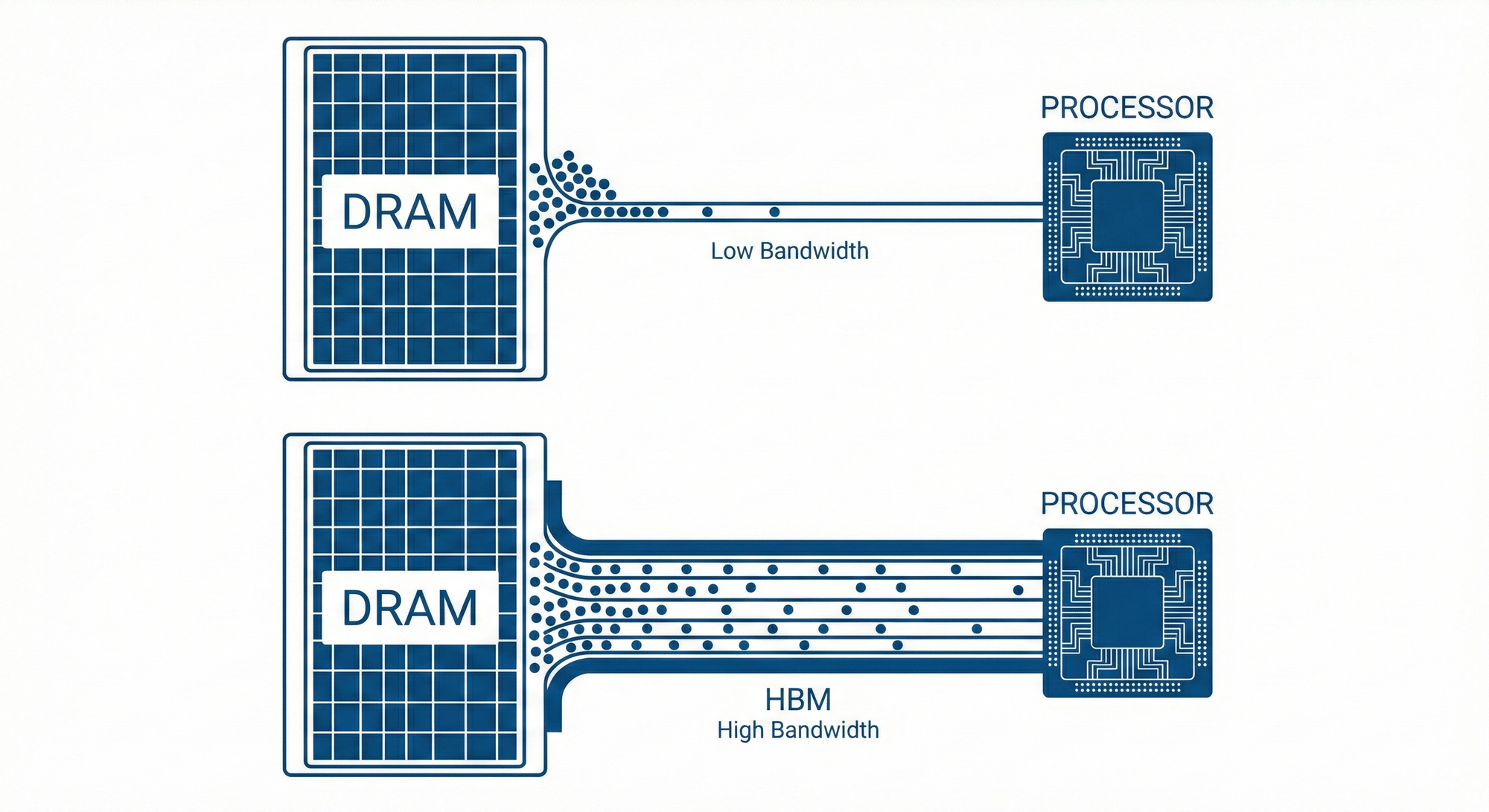
Chapter Two: The Memory Wall — Moving is More Expensive Than Computing
In the AI era, the limitation on computing power is often not that the chip isn't fast enough, but that data cannot be fed to the chip quickly enough. This is the famous "Von Neumann Bottleneck."
Physics tells us a brutal truth: the energy consumed to move data from external memory to a computational unit is approximately 100 to 200 times that required for a single addition operation. In other words, AI chips spend most of their time and power not on "thinking," but on "moving memory."
1. GPU's Anxiety and HBM's Salvation
Because GPUs must handle various unknown tasks, they frequently read from and write to external memory. To alleviate this bottleneck, NVIDIA adopted HBM (High Bandwidth Memory).
HBM vertically stacks DRAM like a skyscraper and then uses advanced packaging (CoWoS) to tightly integrate it next to the GPU, attempting to shorten the data transfer distance. While HBM is extremely fast, it is exceedingly expensive, generates significant heat, and its production capacity is limited (constrained by SK Hynix and TSMC's capacities). This has become a major drawback for GPUs in expanding their computing power.
2. ASIC's Revolution: SRAM Compute-in-Memory
ASIC designers, knowing exactly what models they need to run (e.g., specifically running Llama 3), can adopt a more aggressive strategy: "de-HBM-ization."
Take Groq, a fast-rising Silicon Valley startup, as an example. Its LPU (Language Processing Unit) architecture completely abandons external DRAM/HBM. Instead, it directly fills the entire chip with expensive but extremely fast SRAM (Static Random-Access Memory), integrating it with the computational units.
Result: Its memory bandwidth reaches an astonishing 80TB/s (more than 20 times that of the H100).
Cost: SRAM capacity is very small, unable to store ultra-large models.
Strategy: The capacity problem is solved by chaining hundreds of chips together. This allows ASICs to exhibit ultra-low latency, unattainable by GPUs, in "inference" scenarios—especially for real-time speech conversations.
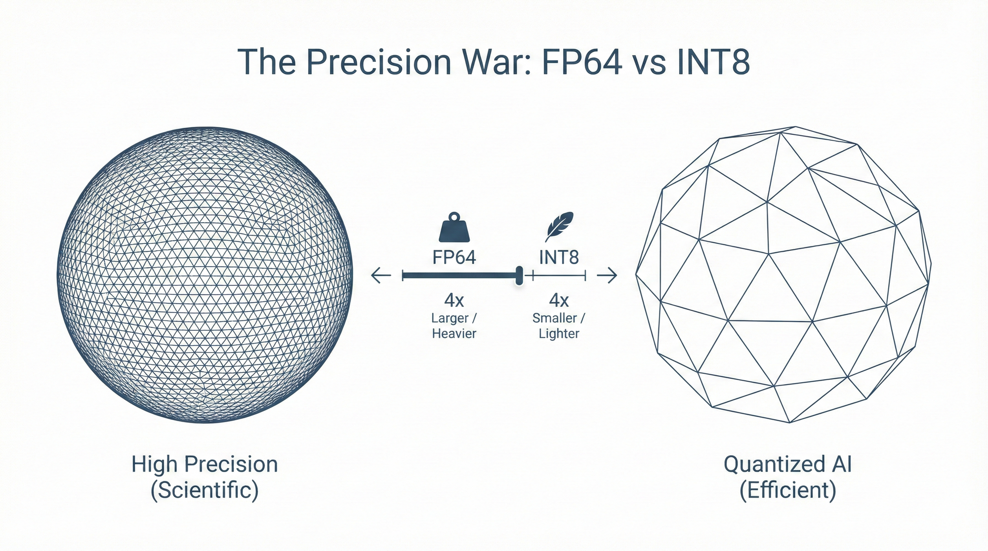
Chapter Three: The Precision War — Mathematical Compromise and "Good Enough"
The GPU's burden lies not only in its architecture but also in "mathematical precision."
NVIDIA's GPUs were originally designed for High-Performance Computing (HPC) tasks, such as simulating nuclear explosions, predicting climate, or developing new drugs. These tasks demand extremely high precision, thus GPUs must natively support FP64 (double-precision floating-point numbers). This means the chip circuitry must be able to handle minute differences up to 15 decimal places.
However, AI neural networks are inherently "fuzzy." They are probabilistic models. When AI tells you that an image is a cat, whether the confidence level is 99.12345% or 99.1% makes absolutely no difference for the end application.
【ASIC's Quantization Magic】 ASIC designers boldly cut support for FP64 and even FP32, focusing on INT8 (8-bit integers) or even FP4.
Data Volume Drastically Reduced: From FP32 to INT8, the data volume becomes 1/4 of the original. This means the same memory bandwidth can transmit 4 times more data.
Circuit Simplification: The multiplier circuits for processing INT8 are tens of times smaller than those for FP64 and consume tens of times less power.
This is why Amazon's Inferentia or Google's TPU can achieve costs that are a fraction of a GPU's when handling inference tasks. They are selling not "perfect mathematics" but "good enough intelligence."
Technical Summary Comparison:
This post is for subscribers only
Sign up now to read the post and get access to the full library of posts for subscribers only.