Preamble: This isn't a chip war; it's a war of physics
In Wall Street earnings calls, analysts discuss gross margins, days of inventory, and AI penetration rates. But in the minds of Jensen Huang and Lisa Su, the enemy they wake up to every day isn't each other, but Physics.
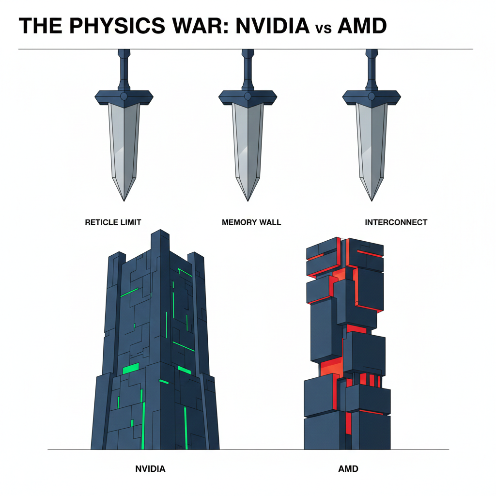
To understand the semiconductor landscape beyond 2026, you must first comprehend the "Three Swords of Damocles" hanging over these two companies. These three physical demons will dictate the technological trajectory and investment opportunities of the next decade:
1. Reticle Limit
ASML's lithography machines have a maximum scanning area of approximately 858 mm² per pass. This is like a printer with a fixed paper size; you cannot print a pattern larger than the paper. However, in the pursuit of computing power, chips need to grow indefinitely.
2. Memory Wall
Over the past 20 years, chip processing speed has increased 90,000-fold, but memory bandwidth has only increased 100-fold. This is like driving a Ferrari on a congested city avenue – no matter how good the engine, it's useless.
3. Interconnect Bottleneck
When one chip isn't enough, and tens of thousands need to compute together, the "communication" between chips becomes the biggest bottleneck. The power consumption of data transfer can even exceed the power consumption of computation itself.
All the powerful tools in the hands of NVIDIA and AMD—CoWoS, HBM, NVLink, Chiplet, SoIC—are forged to slay these three demons.
🦖 Part One: NVIDIA — The Aesthetics of Brute Force and the Game Against Physical Limits
In the world of semiconductors, there are two ways to expand: one is Scale-out (horizontal expansion), like an army of ants moving house, stacking countless ordinary small chips; the other is Scale-up (vertical expansion), like building a Hulk, creating a single, powerful super-individual.
Jensen Huang is an absolute believer in Scale-up. His ultimate goal is singular: to make software engineers feel no "hardware boundaries." Even if the underlying hardware is as complex as alien technology, at the software level, it must appear as an infinitely large single chip.
To realize this ambitious vision, NVIDIA must sequentially slay the demons set forth by physics.
Chapter One: Hopper (H100) — A Philosophical Shift: Learning to "Squint at the World"
The H100 is known as the "Holy Grail" of generative AI, but its greatness lies not in the number of transistors it packs, but in how it changed the values of computer computation.
Before the H100, supercomputers (HPC) were used for tasks like simulating nuclear explosions and predicting climate. These tasks demanded absolute precision, requiring FP64 (double precision) or FP32 (single precision). This is akin to reading with a microscope, where you must discern every fiber on the paper—precise, but extremely slow.
However, an AI neural network is essentially a probabilistic model. It doesn't need to know if the answer is 1.0000001; it just needs to know if "this is likely a cat" or "likely a dog."
The H100 introduced a revolutionary architecture: the Transformer Engine.
This is like an automatic gearbox in a sports car. The chip's internal "traffic police" constantly monitors data flow:
- When encountering critical data that determines the model's core logic, it switches to "microscope mode (FP16/FP32)" to ensure precision.
- When encountering massive volumes of weight fine-tuning data, it instantly switches to "speed-reading mode (FP8)," using only 8 bits to record it.
💡
Physical Significance and Commercial Profit: FP8 data volume is only one-fourth of FP32. This means that on a road of the same width (memory bandwidth), the H100 can handle 4 times the data traffic.
Chapter Two: Blackwell (B200) — Challenging the Reticle Limit with "Conjoined Twin Stitching"
By 2024, NVIDIA hit a wall: the Reticle Limit.
ASML's lithography machines have a maximum scanning area of approximately 858 mm² per pass. Single chips can no longer be made larger, but customer demand for computing power is limitless.
What to do? Jensen Huang's answer: If I can't make one giant carpet, I'll buy two carpets of the maximum size and sew them together side by side.
This is the essence of Blackwell B200—two 800mm² chips forcibly stitched together.
1. CoWoS-L: Nanometer-Scale Subway Engineering
"Stitching" sounds simple, but on a silicon wafer, it's a hellish challenge. If you merely place two chips on a substrate, signal transmission between them will suffer delays, and software will realize, "Oh! These are two separate chips," breaking the magic of Scale-up.
To overcome this, NVIDIA partnered with TSMC, leveraging CoWoS-L (Local Silicon Interconnect) technology.
- No Full Foundation Layer: Traditional CoWoS-S involves laying a complete silicon interposer layer underneath, which is too expensive and fragile.
- Building Only a Subway: CoWoS-L instead uses an organic substrate (RDL) as the foundation, but at the "seam" where the two chips need to communicate, it precisely embeds a "silicon bridge (LSI Bridge)."
This LSI Bridge acts like a nanometer-scale subway connecting twin towers.
Through the NV-HBI (High Bandwidth Interface), the communication speed between the two chips reaches 10 TB/s. This speed is so fast that while physically they are two chips, in the world of electronic signals, they "don't know" they are separate. Software believes it is still accessing the cache of a single chip.
This is the secret behind the B200 having 208 billion transistors, yet operating like a single chip.
2. FP4: The Brute Force of Inference with "Reading Ten Lines at a Glance"
With the B200, NVIDIA pushed the "fuzzy philosophy" to its extreme, supporting FP4 (4-bit) precision.
This means it uses only 4 bits (0000 to 1111, with only 16 variations) to represent a number. While this is too coarse for humans, it's just enough for trained AI models (inference stage).
This dramatically boosts the B200's inference capabilities, making it a killer feature for commercial deployment.
Chapter Three: Blackwell Ultra (B300) — The Perfect Patch to Fill Strategic Gaps
While powerful, the B200 initially faced two fatal weaknesses: low CoWoS-L yield rates and inferior memory capacity compared to AMD. To counter its rival, NVIDIA introduced a tactical revision: the B300 series.
1. B300 (GB300): Memory's Revenge — HBM3e 12Hi
AMD's MI300X, thanks to its Chiplet architecture, packed 192GB of memory, making the 192GB B200 appear insufficient.
The B300's counter-strategy is "adding floors to the library."