In the dazzling constellation of Taiwan's semiconductor industry, the spotlight invariably follows TSMC (the king of manufacturing) and MediaTek (the titan of computing). By comparison, Novatek Microelectronics Corp. (Novatek) is like a recluse in simple engineer's attire. It rarely holds major press conferences, its management seldom grants media interviews, and even when its share price surged past NT$600, market discussions about it remained at the superficial level of "high dividend yield" and "cyclical display driver IC stock."
However, this is a profound misunderstanding.
💡
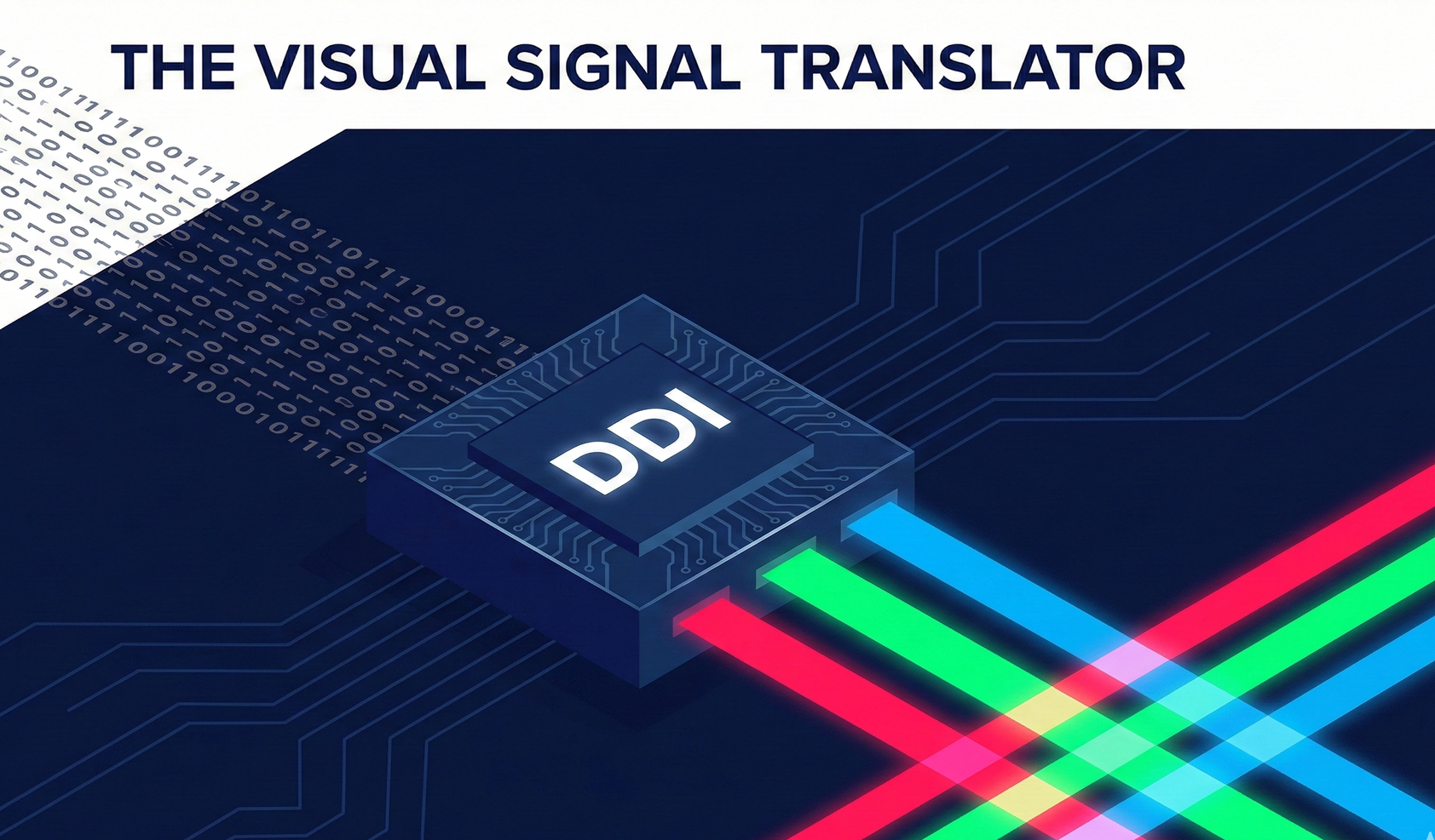
Analogy of the Digital World as an Organism: CPU/GPU (e.g., Intel/NVIDIA): The "brain," responsible for logic operations and content generation 5G/WiFi (e.g., MediaTek/Broadcom): The "nerves," responsible for transmitting signals DDIC (Display Driver IC, Novatek): The "translator for the optic nerve and retina"
Imagine your iPhone 15 Pro screen, with approximately 2.7 million pixels (2556x1179 resolution). In an instant of 1/120 second (120Hz refresh rate), it must precisely command these 2.7 million tiny lights to illuminate in different colors and display varying brightness levels. Furthermore, it needs to perform Gamma correction, color gamut mapping, and even repair physical defects in the panel itself, all while accounting for the persistence of vision in the human eye.
Without Novatek's chips, even NVIDIA's most powerful H100, no matter how strong its computing power, would only generate unseen binary code; and Apple's clearest photos would appear as nothing more than a blank, dark screen.
Novatek controls the "last mile" of the human-machine interface (HMI).
In the past, the market considered display driver ICs to be a commodity, a red ocean driven by price competition. But with the rise of OLED, VR/AR, and automotive cockpits, display driver ICs are undergoing a qualitative transformation—evolving from mere "on/off control" to "AI image quality engines" capable of edge computing.
🎯
Core Thesis of This Report: This report will take you through Novatek's 27-year history, dissecting how this company has built the deepest technological moat with the most conservative financial discipline. We will demonstrate that: Novatek is not an accessory to the panel industry; it is the definer of visual computing.
Chapter 1: Noble Origins and the "Farmer's Philosophy" (1997-2010)
"In the semiconductor industry, there are two ways to survive: one is to constantly hunt for new prey like a pack of wolves (through M&A), like MediaTek; the other is to cultivate gold from barren land like a farmer, and that is Novatek."
1.1 The "Second-Born" Prince of the UMC Spinoffs
1997 was a pivotal year for the structural transformation of Taiwan's semiconductor industry. Robert Tsao, then chairman of United Microelectronics Corporation (UMC), decided to implement a "vertical specialization" reform, spinning off its internal IC design departments to transform UMC into a pure-play foundry. This decision led to the birth of the renowned "UMC Family."
In the list of spinoffs at the time, resource allocation was not egalitarian:
The Eldest Son: MediaTek — Formerly the "Multimedia Department," it focused on optical disc drive chips, which were highly popular at the time, essentially born with a silver spoon.
The Second Son: Novatek — Formerly the "Commercial Products Department," its main products were keyboard and mouse controller chips.
Compared to MediaTek's high technological barriers and high gross margins, Novatek started with businesses typically considered "computer peripheral sundries." These products had low technical content and high price sensitivity, and were initially seen as thankless tasks.
This starting point of "resource scarcity" and "razor-thin margins" shaped Novatek's corporate DNA to be distinctly different from MediaTek's:
MediaTek — Tends to trade capital for time, daring to invest heavily in acquisitions (e.g., buying MStar, Ralink).
Novatek — Developed a character of "extreme cost control" and "organic growth."
Even after its annual revenue exceeded NT$100 billion, Novatek maintained extremely low employee turnover and exceptionally high R&D efficiency (revenue per employee). They were accustomed to making every dollar count, and this frugality became their strongest shield in the fierce competition that followed.
1.2 First Transformation: The Century Opportunity of LCD and "Import Substitution"
In 1999, Novatek's current chairman (then general manager) Steve Wu made one of the most important decisions in the company's history: to enter the LCD Large Driver IC (LDDI) market.
The backdrop at the time was a century-long migration in the global display industry from CRT (cathode ray tube) to LCD (liquid crystal display). The Taiwanese government promoted the "Two Trillion & Two Stars" program, and panel manufacturers like AUO and Chimei were aggressively building new fabs. However, the chips required to drive these panels were then almost 100% controlled by major Japanese manufacturers (Toshiba, NEC, Sharp, Epson).
Japanese manufacturers' chips were high-quality but extremely expensive, and their delivery times were inflexible. Taiwanese panel manufacturers had ample production capacity but were constrained by Japanese chips.
Novatek identified this huge gap for "import substitution."
1.3 Novatek's Winning Formula: Close Foundry Ties
Why Novatek? At the time, there were over a dozen Taiwanese companies making driver ICs (e.g., Himax, Raydium, FocalTech), so why did Novatek dominate?
The key lay in UMC's (its "rich father") production capacity support and a special process technology.
Display Driver ICs (DDIs) differ fundamentally from general logic chips in one aspect: High Voltage (HV).
CPUs operate at just 1V.
Driving liquid crystals to rotate requires 10V ~ 20V.
This means you cannot use standard processes to make DDIs. You need to grow a special "thick oxide layer" on the wafer to withstand high voltage.
Novatek collaborated closely with UMC to jointly develop a special HV (High Voltage) process:
Cost Advantage — Novatek utilized UMC's older 8-inch fabs, whose depreciation was fully accounted for, resulting in costs far lower than Japanese manufacturers still using dedicated production lines.
Capacity Guarantee — When the panel market was booming and experiencing severe shortages, UMC prioritized supplying its "favored offspring" Novatek. This compelled panel manufacturers like AUO and Chimei to purchase Novatek's chips to ensure their material supply.
🏆
Result: By the mid-2000s, Novatek rapidly swept the market with a strategy of offering "half the price of Japanese competitors, with 90% of their performance." By 2010, Japanese display driver IC manufacturers had almost completely exited the standard LCD market, and Novatek ascended to become the global leader.
1.4 Unique Leadership Style: The Silent Executor
To understand Novatek, one must understand its spiritual leader, Steve Wu.
Unlike Ming-Kai Tsai (MediaTek), who enjoys discussing strategies, S-curves, and industry trends, Steve Wu is extremely pragmatic and rarely speaks of grand narratives.
📊
Among institutional investors, Novatek is often described as: "This company offers no surprises, but it will never give you a shock either." Novatek's financial guidance accuracy is astonishingly high. This reflects the management's micrometer-level precision in controlling its supply chain, inventory, and customer demand.
This "farmer's philosophy"—not relying on luck, but diligently cultivating the land to ensure every seed (R&D investment) yields a harvest (profit)—has allowed Novatek to remain profitable and never incur losses through multiple crises, including the 2008 financial crisis and the rise of China's red supply chain in 2015.
Chapter 2: The Physical Moat of DDI — Why Can't Chinese Manufacturers Kill It?
"In the world of digital chips (like CPUs), you can bridge the gap by buying IP and advanced processes. But in the world of analog chips (like DDIs), the laws of physics are the only judge. You cannot fool current with code, nor can you solve high voltage with Moore's Law."
There's a common misconception in the market that display driver ICs (DDIs) are "low-tech" products. The reason is simple: they don't require 3nm processes like CPUs, nor do they need to run AI models like GPUs.
However, DDIs are, in fact, "hybrid monsters" of analog and digital. Their design challenge lies not in miniaturization, but in "control."
2.1 Microscopic Anatomy of a DDI: The Art of Conducting a Pas de Deux
To understand the difficulty of DDIs, let's first grasp how a screen works.
Current screens (whether LCD or OLED) are essentially giant matrices. For a 4K screen, for example, it has 3840 (columns) x 2160 (rows) x 3 (RGB) = approximately 24.88 million sub-pixels.
To operate all these 24.88 million switches in 1/120 second (8.3 milliseconds), Novatek has designed two elite forces:
1. Gate Driver — The "Roll Call Officer"
Responsibility: Controls the switches for each "row."
Action: It must scan rapidly from top to bottom, like a machine gun.
$T=0$ microseconds: Open the gate for row 1 (Gate On).
$T=10$ microseconds: Close row 1, open row 2.
And so on, up to row 2160.
Difficulty:Timing. If it is 0.1 microseconds late, the screen will exhibit tearing or ghosting.
2. Source Driver — The "Coloring Officer"
Responsibility: Fills in the colors for each "column."
Action: The moment the Roll Call Officer announces "row 1 open," the Source Driver must simultaneously supply precise voltages to the 3840 x 3 pixels in row 1.
Pixel A to display "deep red" $\rightarrow$ supply 4.5V.
Pixel B to display "light blue" $\rightarrow$ supply 2.1V.
Difficulty:Precision. This is where Novatek excels. The human eye is extremely sensitive to brightness. If Novatek's output voltage drifts by 3 millivolts (0.003V), the user's eyes will perceive "color shift" or "flicker." Delivering such precise analog voltages simultaneously across thousands of channels in an extremely short time is a field often referred to as "black magic" in circuit design.
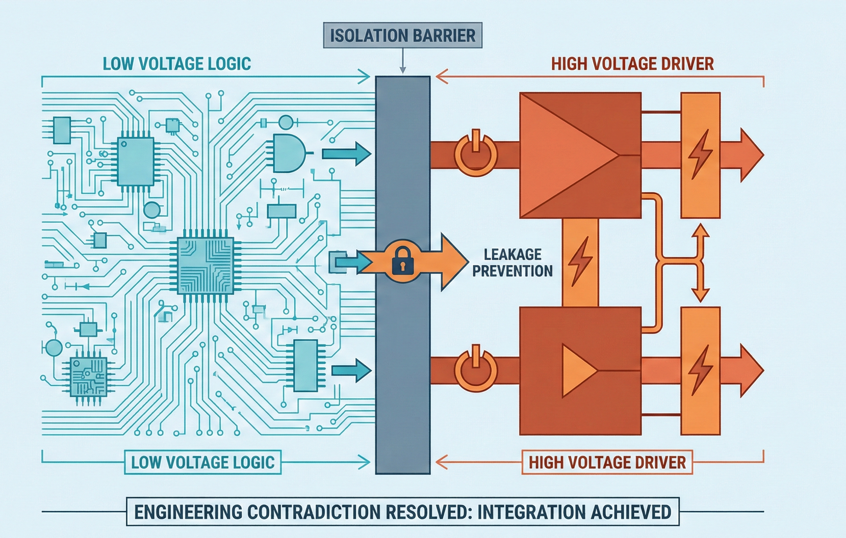
2.2 High Voltage Process (HV Process) — The "Strongman" of the Chip World
This is the largest physical divide between DDIs and general logic chips.
1. Conflict of Physical Logic
CPU/Mobile chips (Logic): Pursue power efficiency and speed. According to the physical formula $P=IV$, lower voltage is better. Advanced processes now push voltages down to 0.7V ~ 0.9V. These transistors are like "sprinters" — fine muscle fibers, fast, but fragile.
Driver chips: Their job is to drive physical structures.
LCD: Requires an electric field to twist the angle of liquid crystal molecules.
OLED: Requires current to drive organic materials to emit light. This needs "strength." DDI operating voltages typically reach 10V ~ 30V. These transistors are like "weightlifters" — tough and powerful.
2. Process Barriers
If you were to take the circuit design of a DDI to TSMC's 5nm production line for CPUs, there would be only one outcome: the chip would burn out instantly upon power-up (Breakdown). Because a nanometer-level insulating layer simply cannot withstand 20V of high voltage.
Therefore, Novatek must use a special manufacturing process: High Voltage Process (HV Process).
This is a "hybrid process":
On the same chip, some areas are designed for 1V low-voltage logic (responsible for computation).
Other areas need 30V high-voltage components (responsible for output).
Complex "isolation layers" and "level shifters" must be designed in between to prevent high voltage from leaking and burning out the low-voltage sections.
3. Why is this a moat?
Because this process has "no standard answer."
TSMC's 5nm logic process is standardized; anyone can submit a design for production with similar results. But the HV process requires IC design houses (like Novatek) and foundries (like UMC) to spend a decade "fine-tuning parameters."
What should be the doping concentration?
How thick should the oxide layer be?
How is heat dissipation managed?
This forms a closed ecosystem. Although new Chinese design companies (like InnoLux) receive government subsidies and can afford IP, they cannot find foundries that offer HV parameters as finely tuned as those developed by Novatek and UMC over twenty years. This results in their chips having "large area, high heat generation, and low yield."
2.3 The Black Magic of Analog Design — Noise and Interference
Digital circuits are a world of 0s and 1s, with tolerance (0.9 is 1, 1.1 is also 1).
Analog circuits are a continuous world, with no tolerance (10.0V is 10.0V, 10.1V is wrong).
Within the small chip space of a DDI, both simultaneously exist:
High-speed switching digital signals (switching hundreds of millions of times per second, generating significant noise).
Extremely sensitive analog voltages (responsible for displaying colors).
This is like asking an embroidery artisan (analog signal) to keep a steady hand in a room hosting a heavy metal rock concert (digital noise).
Novatek's True Strength: Noise Immunity Design
Novatek's engineers are masters at laying out clean circuits (Layout) in such extremely harsh electromagnetic environments. They know which lines to route around, where to add shielding, and where to place capacitors for filtering.
This kind of experience cannot be learned from textbooks; it can only be accumulated through countless failed tape-outs. This is why Novatek's senior engineers command extremely high salaries, because their intuitive layout skills are a company asset.
2.4 Why Can't Chinese Manufacturers Kill It?
Since 2015, the Chinese government has heavily supported the semiconductor industry, and BOE has already dominated the global panel industry. Logically, Chinese driver IC manufacturers should have capitalized on this to replace Novatek.
However, the reality is:
In the mid-to-low-end LCD market, Chinese manufacturers did indeed grab market share; but in OLED, automotive, and high-end gaming segments, Novatek's market share has actually increased instead of decreased.
The reason lies in "Yield" and "Power Consumption."
Low-end battlefield: Screen resolution is low, requiring less voltage precision, and heat generation is less of a concern. Chinese manufacturers can compete on price with subsidies.
High-end battlefield (e.g., iPhone):
Extremely narrow bezels: Chips must be extremely small (COP packaging).
Power-saving requirements: Apple demands extreme power efficiency.
Yield pain point: If the DDI yield is only 90%, it means one out of every 10 iPhones will have incorrect screen colors, which would be catastrophic for Apple.
Novatek, with its mature HV process and analog design capabilities, can produce chips that are 10% smaller and 15% lower in power consumption than competitors, with a first-pass yield close to 99%.
For Apple and Samsung, it is simply not worth risking unstable Chinese chips to save $0.5 per chip.
Chapter 3: The Algorithm's Counterattack — How Did Novatek Penetrate the Apple Supply Chain?
"Perfect hardware does not exist. In nanoscale manufacturing, variation is absolute, consistency is relative. Novatek's greatness lies in acknowledging the imperfections of the physical world and using mathematical algorithms to fabricate a perfect digital world."
In 2017, Apple released the iPhone X, the first iPhone to feature an OLED screen.
This was a watershed moment for the display driver IC industry. Before this, LCDs were commodities, and driver ICs merely needed to "light up" the pixels. But the advent of OLED brought a fatal flaw that was almost physically impossible to resolve—Mura.
Novatek's ability to fix this flaw is key to its indispensable role in the iPhone supply chain (even if indirectly supplied through LGD or BOE).
3.1 OLED's Innate Flaw: Mura (Cloudy Patches)
1. From Light Bulbs to Spray Paint: A Manufacturing Revolution
LCD (Liquid Crystal Display): Has a uniform backlight panel (LED bulbs) behind it. This is like uniformly turning on fluorescent lights in a classroom, where brightness is very even.
OLED (Organic Light-Emitting Diode): Each pixel emits its own light. The production process involves spraying organic materials onto a glass or plastic substrate using an "evaporation" machine.
2. Physical Uncertainty
Imagine trying to spray 2.7 million dots on a wall with a spray can and guaranteeing that the paint thickness of each dot is atomically consistent. This is impossible.
Some dots are sprayed thicker, resulting in higher resistance and dimmer light.
Some dots are sprayed thinner, resulting in brighter light.
TFT (Thin-Film Transistor) Variation: The transistors themselves that control the current also have variations in their characteristics (Vth Shift).
3. Result: A Dirty Screen
If you apply the exact same 5V voltage to an OLED panel, the result will not be a pure white screen, but a gray screen with spots of varying shades, looking like a dirty screen or one with a misty haze. This is known in the industry as Mura (Japanese for "unevenness").
For Apple, which strives for perfection, this is an absolutely unacceptable defect. Without a solution for Mura, the yield rate for OLED panels might be less than 10%.
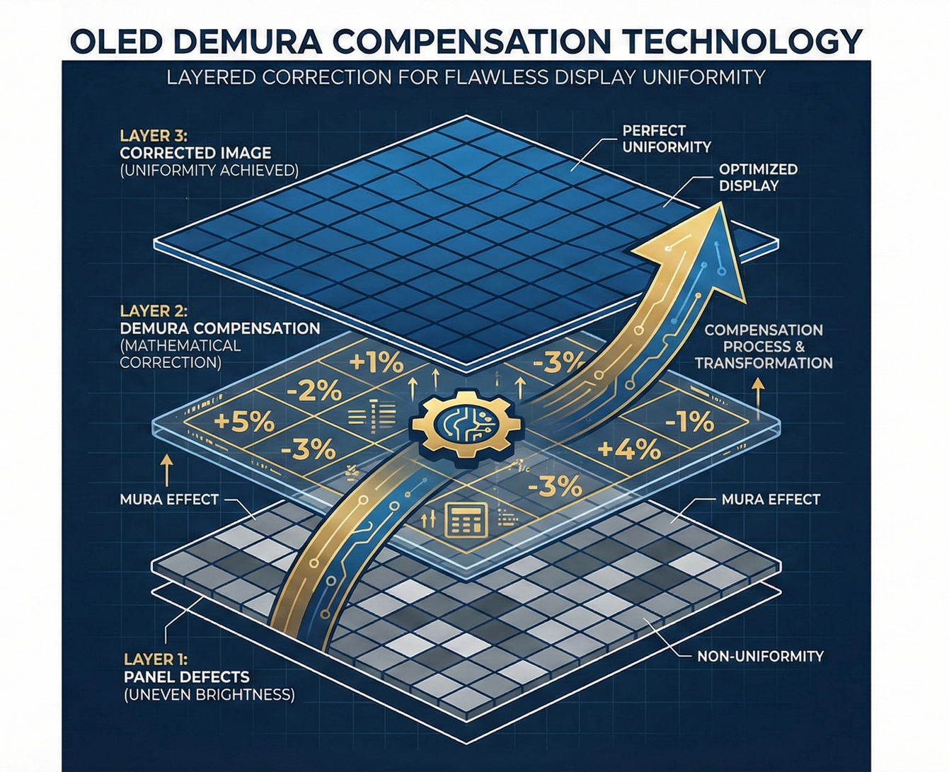
3.2 Key Technology: Demura (Digital Concealer)
Since physical perfection is impossible, Novatek engineers shifted their thinking: "Can we fool the human eye?"
This gave birth to Demura (De-mura, spot removal) technology. This is not a hardware technology; it is a complex system of "detection + computation + compensation."
Before assembly, each iPhone screen in the factory is lit up. High-resolution cameras capture the screen's image, and Novatek's algorithms analyze the brightness characteristics of the 2.7 million pixels.
Pixel A: Inherently flawed, brightness is only 95% of the standard value.
Pixel B: Inherently overactive, brightness is 103% of the standard value.
Step Two: Create a "Compensation Table" (Look-up Table generation)
The system calculates a huge correction table (digital map).
To "save" Pixel A, record "+5% voltage."
To "suppress" Pixel B, record "-3% voltage." This map is burned into the Flash memory (either external or embedded in the chip). This is why high-end OLED DDIs need integrated Flash.
Step Three: Real-time Compensation
This is the most challenging step and demonstrates the computing power of Novatek's chips.
When you are scrolling on your phone, the CPU commands: "Display 100% brightness for all."
Novatek's DDI, a nanosecond before sending out the signal, quickly consults the table:
For Pixel A, it outputs 105% of the voltage (105% x 95% inherent quality $\approx$ 100%).
For Pixel B, it outputs 97% of the voltage (97% x 103% inherent quality $\approx$ 100%).
Result:
Although the panel is physically uneven, your eyes perceive a perfectly uniform image. Novatek acts like a "digital makeup artist," precisely concealing panel imperfections before each frame reaches your retina.
3.3 The Moat of Computing Power: Why Can't Chinese Manufacturers Copy It?
You might ask, "This sounds like just a lookup table method; can't Chinese manufacturers write code?"
The devil is in the details.
1. Massive Data Throughput
The iPhone 15 has a 120Hz refresh rate. This means Novatek's chip must perform 2.7 million lookups, 2.7 million arithmetic operations (add, subtract, multiply, divide), and then convert them into analog voltages and output them, all within 8.3 milliseconds.
Even a slight delay would cause screen stuttering. This requires an extremely optimized digital logic circuit design.
2. Compression Algorithms
A 2.7 million-pixel compensation table is very large, and Flash memory is expensive. Novatek developed proprietary compression algorithms that can store the entire map in an extremely small capacity while ensuring very fast decompression. This involves patented mathematical encoding techniques.
3. Interference in Touch and Display Driver Integration (TDDI)
Modern phone chips not only drive the display but also sense touch.
When Demura is furiously computing compensation voltages, it generates digital noise that can interfere with faint touch signals. Novatek's strength lies in its ability to perfectly stagger "compensation computations" and "touch sensing" on the timeline (time-division multiplexing), preventing them from interfering with each other.
3.4 The Apple Supply Chain Entry Ticket
Apple's display requirements are among the most stringent in the world. They demand not only uniform brightness but also no color shift at extremely low brightness (e.g., when using the phone at night), where Mura is most apparent.
This leads panel manufacturers (Samsung Display, LG Display, BOE) to rely on display driver ICs.
Panel manufacturers have found that if they use cheaper driver ICs, the panel yield rate might only be 60%, with the remaining 40% scrapped (because Mura cannot be corrected).
However, if they use Novatek's driver ICs, combined with Novatek's advanced algorithms, the yield rate can be boosted to 90%.
💰
The economics are clear: Novatek's chip might cost $1 more, but it saves an OLED panel worth $50. This is the underlying logic for why Novatek can penetrate the Apple supply chain—it doesn't sell chips; it sells "panel yield insurance."
3.5 Evolution: From Mobile Phones to VR/AR with OLEDoS
The success of Demura technology has given Novatek great confidence to enter the next battlefield: Micro OLED (OLEDoS).
In VR devices like Apple Vision Pro, pixel density is as high as 3000 PPI, making the Mura problem ten times more severe than in mobile phones. Furthermore, because the screen is so close to the eyes, any defect is magnified.
Novatek is upgrading its Demura technology into an "AI visual enhancement engine."
This will not only compensate for brightness but also use eye tracking to anticipate where the user is looking and perform Foveated Rendering for the gaze point. This marks Novatek's transformation from a "passive signal receiver" to an AI computing company that "actively interprets images."
This post is for subscribers only
Sign up now to read the post and get access to the full library of posts for subscribers only.