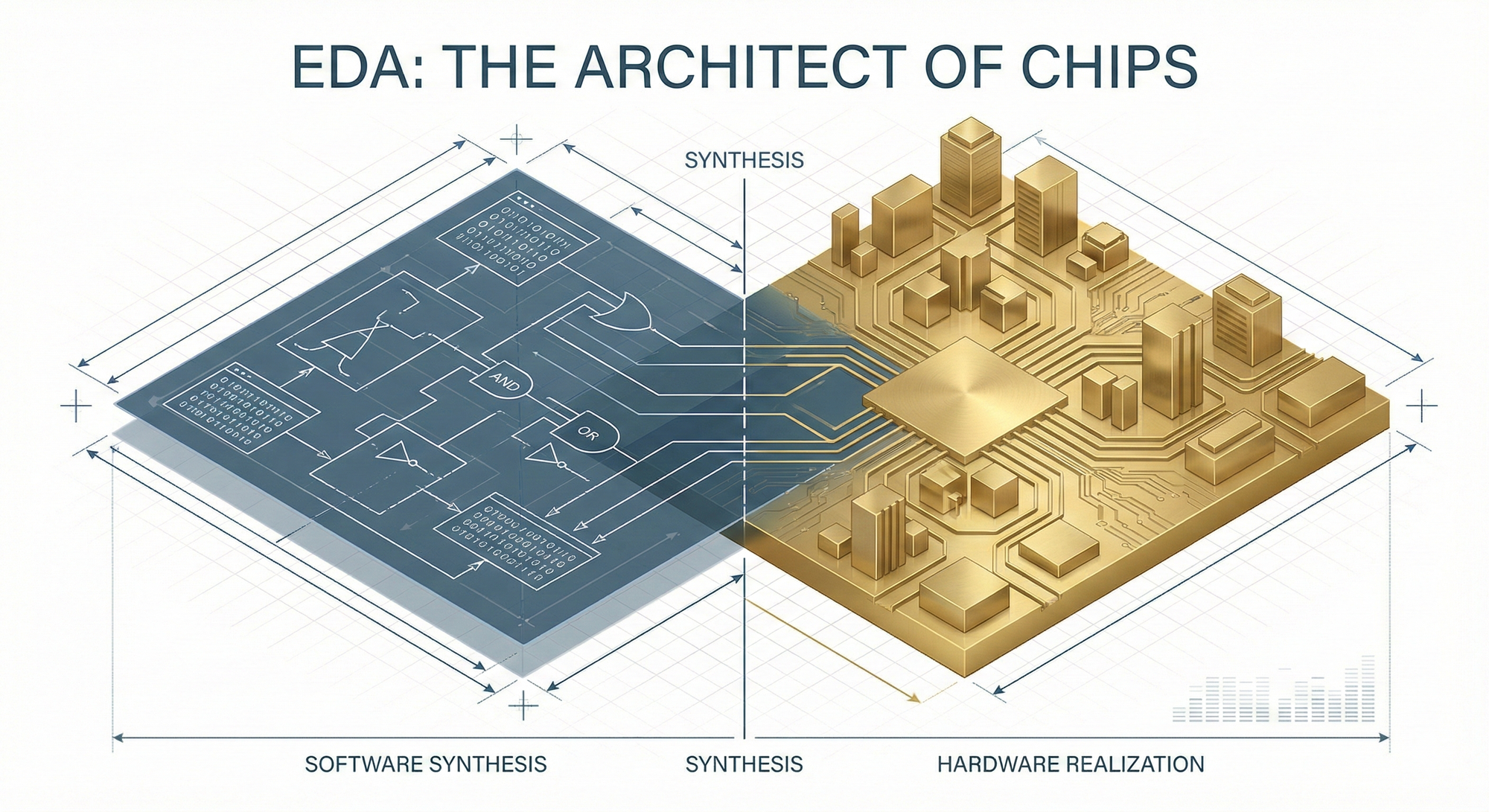
EDA (Electronic Design Automation) is the most upstream and smallest (compared to TSMC's revenue) segment of the semiconductor industry chain, yet it is a critical choke point for the entire industry.
If chip design is likened to constructing a Taipei 101 skyscraper:
- IP (Battleground 1-1) represents prefabricated reinforced concrete modules.
- EDA (Battleground 1-3) is the architect's ultimate CAD system, capable of simulating earthquakes and wind resistance, and automatically calculating structural mechanics.
Without this software, even with the best architects (MediaTek) and the strongest construction companies (TSMC), the skyscraper cannot be built.
Part One: Why is EDA Indispensable?
In the 1970s, when chips contained only a few thousand transistors, engineers could indeed draw circuit diagrams by hand. However, in 2024, the situation is entirely different.
1. Astronomical Complexity
A modern AI chip (such as NVIDIA Blackwell) possesses 208 billion transistors.
- Human Limitations: Manually checking every circuit connection would take centuries.
- Physical Simulation: At the nanoscale, electrical currents generate heat, electromagnetic interference, and signal delays. These physical phenomena must be calculated using complex differential equations before chip manufacturing.
2. The Translator Between Human Brains and Silicon Wafers
EDA is more than just 'drawing software'; it is the sole tool that translates human logic (code) into factory language (mask patterns). It is the core of software-defined hardware.
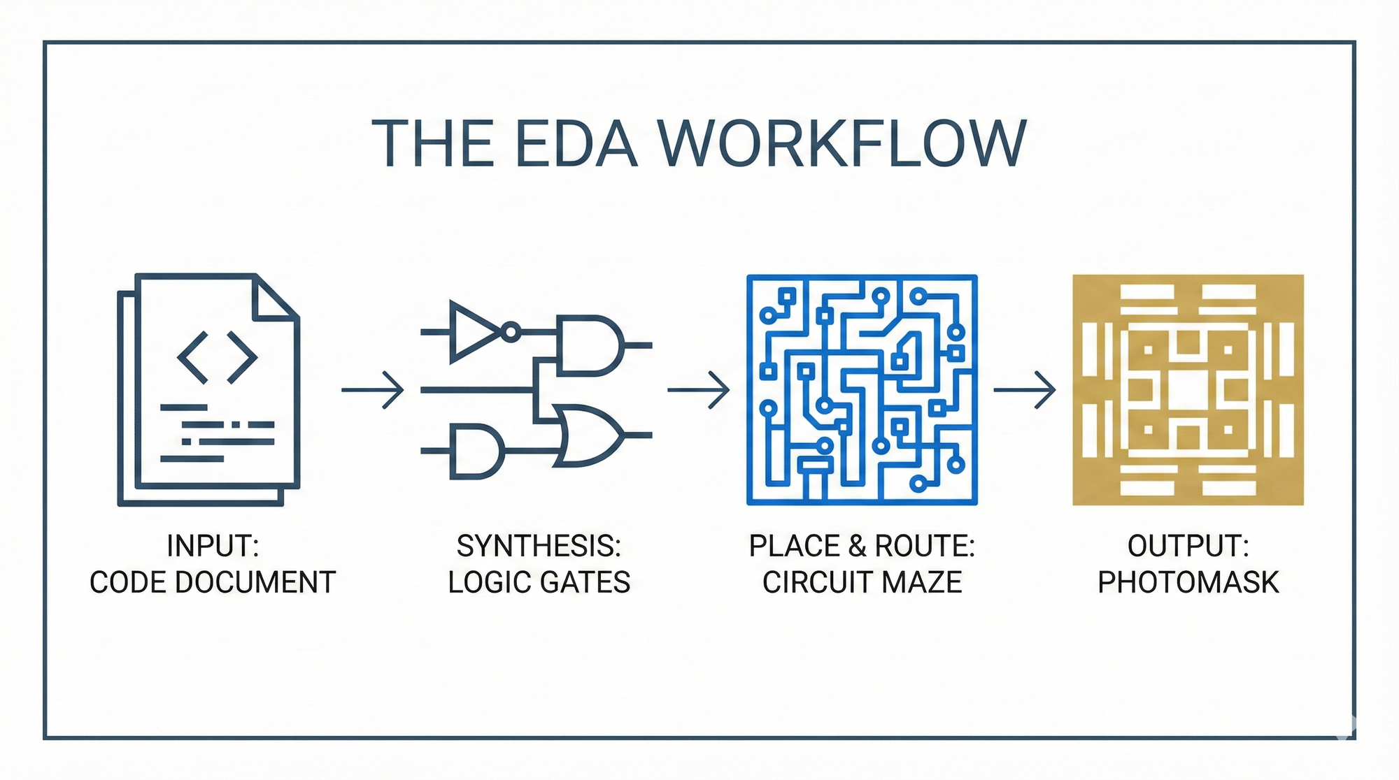
Part Two: The Deep End —— EDA's Core Operations (From Code to Mask)
Investors often assume that designing chips involves drawing, but engineers primarily engage in coding. EDA's value lies in transforming this code into 'gold'. Here are the four critical steps:
1. Logic Synthesis —— Translation
Engineers write RTL code (Verilog/VHDL), for example: 'If signal A is greater than B, output C'.
- EDA's Task: Using a 'synthesizer', it translates this human-readable language into a netlist composed of hundreds of millions of AND, OR, and NOT logic gates.
- Dominant Player: Synopsys' Design Compiler. This is the absolute industry standard, with virtually no rivals.
2. Automatic Place & Route (APR) —— Building the Structure
This is one of the most challenging geometry problems. The software must fit these hundreds of millions of logic gates into a fingernail-sized area and connect tens of billions of metal lines.
- Requirements: Wires must not tangle, paths must be the shortest (for power efficiency), and signals must travel at light speed.
- AI Intervention: Given the astronomical number of permutations, EDA vendors now incorporate AI (such as Synopsys DSO.ai) to explore tens of thousands of arrangements and identify the optimal solution (PPA - Power, Performance, Area).
3. Sign-off —— The Final Verdict
This is a term investors must understand. EDA software plays the role of a 'structural engineer' here.
- DRC (Design Rule Check): Checks for violations of TSMC's rules? (e.g., lines too thin will break, two lines too close will short circuit).
- LVS (Layout vs Schematic): Checks if the drawn layout matches the original design logic?
- Authority: TSMC will only accept an order if the EDA software outputs a Green Light (pass). Without this 'clearance,' the risk of the fabricated chip being scrapped is extremely high, and no one dares to bear the hundreds of millions of dollars in losses.
4. Physical Translation (GDSII & OPC) —— Handover to Photomask
Finally, EDA outputs a GDSII file, which is the chip's 'negative film'.
- Before being sent to the photomask manufacturer, EDA must perform intensive OPC (Optical Proximity Correction) calculations, pre-distorting the patterns (e.g., drawing right angles as dog bone shapes) to offset light diffraction errors.
Part Three: The Moat —— Why is it So Difficult to Replace EDA?
This is a business barrier jointly built by TSMC and EDA vendors, and it's why Synopsys and Cadence stocks command high price-to-earnings ratios.
1. PDK (Process Design Kit) —— The Semiconductor Industry's 'Encrypted Codex'
- Definition: All physical limit parameters for TSMC's 3-nanometer process are packaged into a massive database called a PDK.
- Lock-in: This PDK can only be read by Synopsys and Cadence software.
- Switching Costs: If MediaTek is halfway through designing a chip and wants to switch from TSMC to Samsung, sorry, they would have to start over from scratch. This is because Samsung's PDK is completely different from TSMC's, and the original EDA configuration files are not interchangeable.
2. Hardware Emulation —— The Expensive Refrigerator
This is the fastest-growing business for the two EDA giants in recent years.
- Pain Point: Simulating 200 billion transistors with pure software is too slow; a 1-second computation could take days.
- Solution: Selling clients a **dedicated supercomputer** the size of a refrigerator (e.g., Cadence Palladium, Synopsys ZeBu).
- It's filled with FPGAs or specialized chips, designed to 'act' as the unborn chip.
- This allows NVIDIA's software engineers to develop CUDA drivers on this 'dummy chip' before the actual chip is ready.
- Commercial Value: Each of these machines costs millions to tens of millions of dollars, representing high-value 'weaponry'.
Part Four: Market Landscape and Geopolitics
1. The Three Industry Giants (The Big Three)
Over 90% of the global EDA market is dominated by these three companies. This is a classic oligopoly.
| Company Name | Ticker | Core Strengths | Strategic Position |
|---|---|---|---|
| Synopsys | SNPS | Digital Dominance | The leader. Logic synthesis and sign-off tools are industry standards. The preferred choice for most advanced process digital chips (CPU/GPU). |
| Cadence | CDNS | Analog Powerhouse | The second largest. Extremely strong in analog circuits, mixed-signal, and package layout. Its hardware emulator (Palladium) has a high market share. |
| Siemens EDA | SIE | Verification & PCB | The third largest (formerly Mentor Graphics). Acquired by Siemens, it holds absolute dominance in physical verification (Calibre). |
2. The 'Nuclear Button' of the Chip War (Choke Point)
The most devastating sanction imposed by the U.S. on China's semiconductor industry is not hardware, but EDA.
- GAAFET Ban: The U.S. prohibits the export of EDA software supporting GAA (Gate-All-Around) architecture to China.
- Impact: GAA architecture is required for 3-nanometer processes and below. Without this software, engineers cannot calculate the complex physical fields of 3D transistors.
- Result: This directly blocks competitors' access to 3-nanometer R&D, serving as a precise 'dimension-reduction' strike.
Strategic Summary
- Indispensable: It is the only bridge connecting 'human logic' with 'physical implementation'.
- Deep Moat: Deep integration with foundries (TSMC) through PDKs creates an unshakeable ecosystem.
- Investment Attributes: The EDA industry possesses a dual engine of 'software licensing (high-margin)' + 'hardware emulation (high-growth)', and is less affected by economic cycles (because R&D cannot be cut, even during lean times).
In-depth Research · Quantitative Perspective
Want more insights into semiconductor quantitative research?
[Insight Subscription Plan] Bid Farewell to Retail Investor Thinking: Build Your Alpha Trading System with 'Quantitative Flows' and 'Consensus Data'EDGE Semiconductor Research
📍 Series Map — Navigate the Complete EDGE Semiconductor Research →


