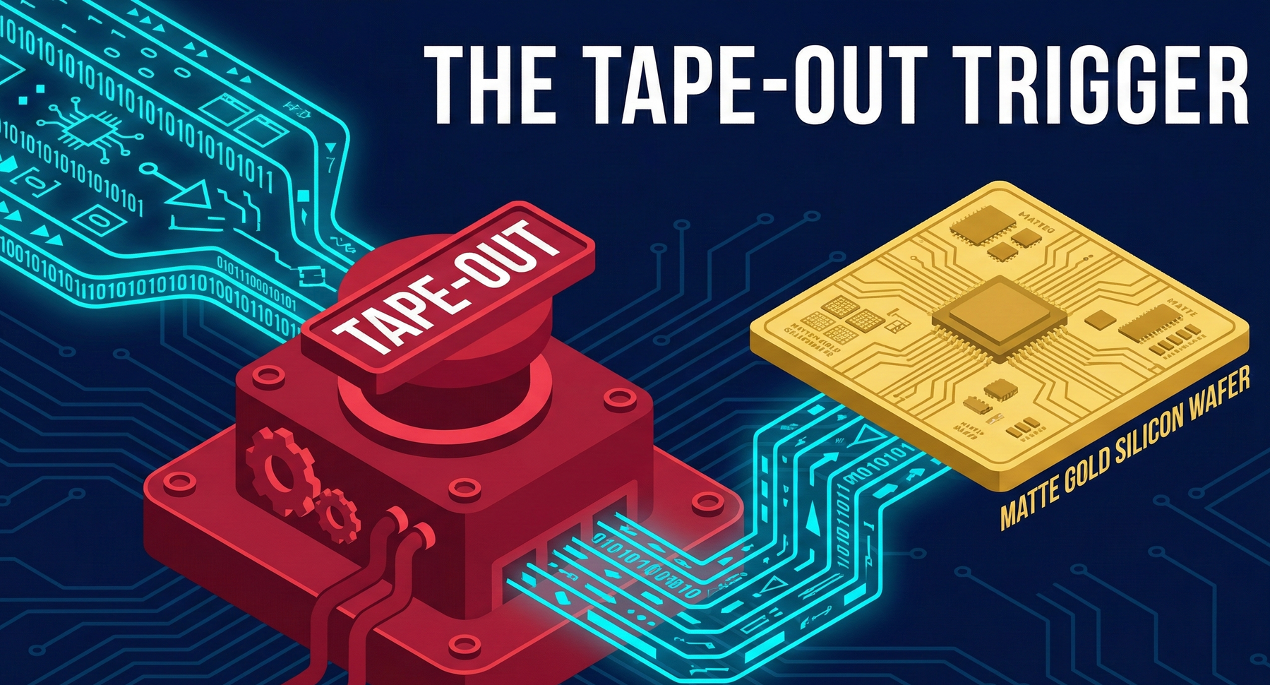
Introduction: Silicon Valley's Most Expensive Button
In the world of software engineering, engineers write code, press "Compile," and see the results in minutes. If there's a bug? No problem, fix it and run it again; the cost is close to zero, at most losing the time equivalent to a few cups of coffee.
In the semiconductor world, however, this action is known as "Tape-out".
This is a term that can make one hold their breath. When the CEO of a chip design company (such as MediaTek or NVIDIA) signs off on a Tape-out, it triggers a series of irreversible chain reactions:
- Massive Capital Evaporation: The cost of creating a "Mask Set" for a foundry (such as TSMC) at the 3-nanometer process node can be as high as $15 million to $20 million USD (approximately TWD 500-600 million).
- Protracted Wait: Chip manufacturing in the factory takes 3 to 6 months.
- Existential Risk: If the chip returns and is found to be non-functional (Dead on Arrival) or performs below expectations, hundreds of millions of New Taiwan Dollars are wasted. Even more critically, you miss the golden window for product launch (Time-to-Market), which could halve your stock price.
To avert this disaster, humanity invented the most complex software system in industrial history: EDA (Electronic Design Automation).
EDA is not merely "drawing software"; it is a "prophet machine of the physical world." Its core value lies in: before a real silicon wafer is etched, creating this chip, which contains 200 billion transistors, "virtually" in the digital world and simulating its entire life cycle.
Part One: Dimensionality Reduction Strike — From Human Logic to Atomic Geometry
The essence of chip design is a translation process from "abstract logic" to "concrete physics." As Moore's Law advances, the difficulty of this translation increases exponentially.
1. Astronomical Complexity
In the 1970s, the Intel 4004 processor had only 2,300 transistors, and engineers could indeed draw circuit diagrams by hand. However, in 2024, a top-tier AI chip (such as NVIDIA Blackwell) possesses 208 billion transistors.
- Scale Analogy: If one transistor is likened to a house, then designing an AI chip is equivalent to planning an architectural complex on a fingernail-sized area that accommodates the equivalent of 20 times the Earth's total population.
- Connection Difficulty: Between these 200 billion "houses," hundreds of billions of "wires" must also be laid. These wires must not be tangled, must not take circuitous routes, and their signal transmission speed must approach the speed of light.
This already exceeds the limits of the human brain, and even the limits of ordinary computers.
2. The Four Acts of Digital Alchemy
How do EDA tools accomplish this impossible task? They break down the process into four key steps.
Step 1: Logic Synthesis — A Distorted Translation
- Input: Engineers write RTL code (Verilog/VHDL). This resembles C language and describes behavior, for example: "If the clock signal rings, add data from A to B."
- Translation: EDA tools (such as Synopsys Design Compiler) translate this "human language" into a "Netlist" composed of logic gates like AND, OR, NOT, and NAND.
- Game: This is not a one-to-one translation but a multi-variable game.
- If you require "high speed," the software will select logic gates with higher leakage but faster response times.
- If you require "power saving," the software will automatically insert "Clock Gating" to shut down inactive circuits.
- Challenge: The software must, within hours, find the optimal solution from hundreds of millions of permutations and combinations that meets PPA (Performance, Power, Area) requirements.
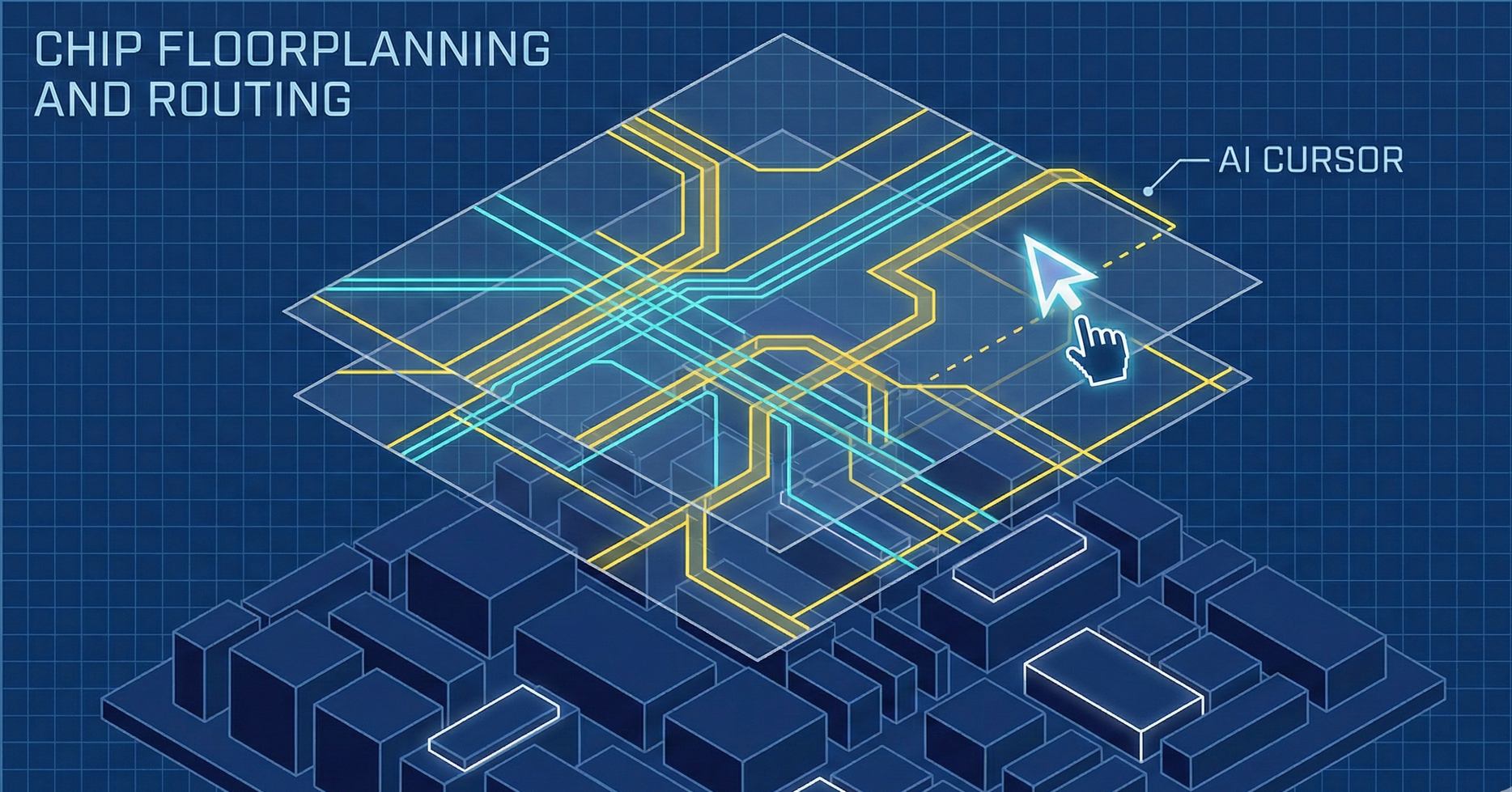
Step 2: Automatic Place & Route (P&R) — Micro-Urban Planning
This is the step with the highest geometric computation volume in the EDA flow.
- Place: Determines where each logic gate should be positioned. Computational units are placed in the center, memory on the sides, and I/O interfaces around the perimeter. This is like planning the location of every building in a city like Tokyo.
- Route: Connects the circuits. The metal lines inside a chip are not planar but three-dimensional, typically having 10 to 15 layers (Metal Layers). EDA software must perform 3D maze routing calculations.
Physics' Revenge: Before 7 nanometers, traces could still be considered ideal conductors. However, at 3 nanometers, traces become extremely thin, causing resistance (R) to sharply increase; if two lines are too close, capacitance (C) effects are generated. These "Parasitics" can lead to signal delays. EDA tools must calculate these physical effects in real-time while routing. If a line is found to have too high a delay, it must be immediately "torn down and rebuilt" to find a new path.
Note: This is why EDA vendors are now adopting AI (such as Synopsys DSO.ai) — because human-defined rules have been exhausted, and only AI can find more optimal solutions in the geometric maze.
Part Two: Verification and Simulation — Why Buy a "Giant Refrigerator"?
If the steps above were about "building a house," then Verification is about simulating whether "this house can withstand earthquakes, fire, and riots." This is the most expensive and time-consuming stage before Tape-out, occupying approximately 60%~70% of the entire chip development cycle.
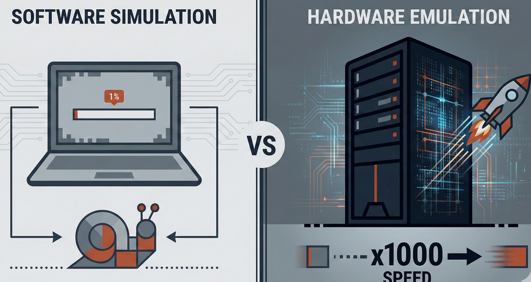
1. The Limits of Software Simulation
Traditionally, engineers use software (simulators) to run tests.
- Pain Point: The speed is too slow. Simulating 1 second of actual operation for a modern GPU (e.g., booting an OS, running a game segment) using pure software simulation on high-performance servers can take several weeks.
- Consequence: Software teams cannot wait. NVIDIA's CUDA driver developers cannot wait two years for a chip to be manufactured before starting to write code, as that would significantly delay the product's market launch.
2. The Expensive "Giant Refrigerator" (Hardware Emulation)
To solve the speed problem, EDA vendors introduced hardware emulators, which resemble giant server racks, such as Cadence Palladium or Synopsys ZeBu.
- Principle: Using chips to "act out" chips. These machines are filled with thousands of specialized processors or FPGAs. They can map your designed 20 billion transistor circuits onto the internal hardware of the machine to perform parallel computations.
- Capability: Speeds are 1,000 to 10,000 times faster than pure software simulation.
- Value: This allows software engineers to boot an OS, run games, and test AI models on this machine before the "chip is even born."
- Cost: One of these machines can cost millions to tens of millions of US dollars. It is one of the most expensive assets in a semiconductor R&D center, typically housed in a temperature and humidity-controlled glass room, receiving absolute VIP treatment.
Part Three: Sign-off and Optics — The Final Judgment
When the design is complete and simulations pass, is it finally ready to be sent to TSMC? Not yet. The final hurdle involves two extremely computation-intensive processes.
1. Sign-off — The Foundry's Admission Ticket
TSMC will not accept your design blueprints casually unless you present a "certificate of qualification." This is Sign-off.
- DRC (Design Rule Check): TSMC's 3-nanometer process has a "codebook" thousands of pages thick, stipulating physical limits. For example: "metal line width cannot be less than X nanometers," "right-angle turns must have chamfers." EDA software must scan the entire design to find any rule violations.
- LVS (Layout Vs Schematic): Checks if the drawn geometric layout matches the original logical circuit design.
Why is it important? If DRC rules are violated, the chip might break, short circuit, or have extremely low yield during manufacturing. Without an "Clean" (error-free) report generated by EDA software, TSMC will absolutely not allow the mask factory to begin production.
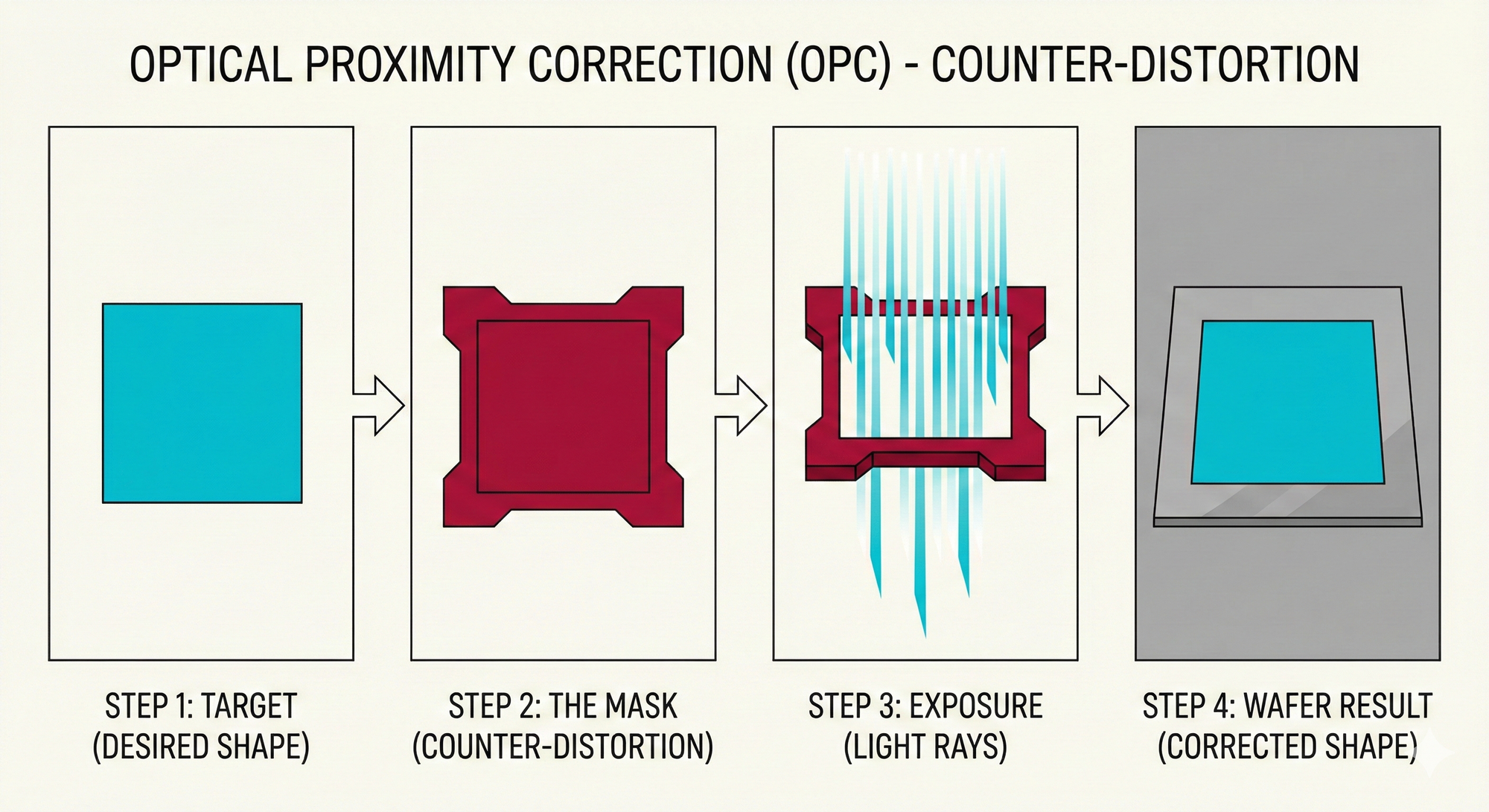
2. OPC (Optical Proximity Correction) — The Black Magic of Optics
This is the final and most computationally intensive step in the Tape-out process.
Physical Dilemma: The wavelength of the light source (DUV) we use for exposure is 193 nanometers, but the lines we want to draw might be only a few tens of nanometers. What happens when you use a very thick marker (light) to draw very thin lines? The answer is Diffraction. The light will blur, square corners will become rounded, and two closely spaced lines will merge together.
Brute-Force Solution: To counteract this physical phenomenon, EDA software must "pre-distort" the patterns.
- If you want a perfect square, what is drawn on the photomask might be a "dog bone" shape (with four outward-protruding corners). This way, after the light blurs, it will perfectly form a square.
- Computational Black Hole: This requires complex optical inverse computations for hundreds of billions of patterns across the entire wafer. This is one of the largest single industrial software computational tasks on Earth. Just running this one layer of OPC can take thousands of servers working day and night for several days.
Conclusion: Why is Tape-out so Expensive?
Returning to the core question of this chapter: why does pressing the Tape-out button cost so much?
Superficially, you pay TSMC for mask manufacturing. In reality, that several hundred million New Taiwan Dollar cost includes massive "hidden costs":
- Computational Power Costs: To run Synthesis, APR, and OPC, you need enormous server farms.
- Software Licensing Fees: EDA tool licenses are typically annual, with a full-flow tool suite often costing millions of US dollars.
- Hardware Emulation Costs: The expense of purchasing or leasing a "giant refrigerator."
- Risk Premium: To ensure that the fingernail-sized silicon chip functions perfectly the moment it's powered on, the entire industry chain invests astronomical resources in "predicting the future."
If EDA were an architect's CAD software, it would certainly not be just for drawing. It is used to simulate earthquakes, pre-enact fires, calculate the stress on every steel bar, and ensure that we have already "lived" in the building for a year before it is even constructed.
This is the essence of EDA: it is the sole bridge connecting human logic with physical implementation, and it is the most expensive and indispensable leverage in the semiconductor industry.
In-depth Research · Quantitative Perspective
Want more insights from semiconductor quantitative research?
[Insight Subscription Plan] Bid Farewell to Retail Investor Mentality: Build Your Alpha Trading System with 'Quantitative Capital Flows' and 'Consensus Data'EDGE Semiconductor Research
📍 Series Map — Navigate the Complete EDGE Semiconductor Research →


