Foreword: The 30-Year War Between "Real Men" and "Smart Ones" (The War of Models)
In the 1980s, a famously macho quote circulated in Silicon Valley, from AMD founder Jerry Sanders:
"Real men have fabs."
This statement precisely captured the truth of that era. In the early days of semiconductors, the strong players had to be IDMs (Integrated Device Manufacturers). You had to design your own blueprints, build your own factories, and tune your own machine parameters. The tight coupling of design and manufacturing was seen as the best guarantee of performance. Fabless design companies, which didn't own factories, were ridiculed as mere paper strategists who could only draw pictures.
However, in 1987, a 56-year-old Chinese-American engineer in Hsinchu, Taiwan, proposed an idea that seemed humble and unconventional at the time:
"I don't want to be a hero; I want to be everyone's servant."
Morris Chang founded TSMC (Taiwan Semiconductor Manufacturing Company) and invented the Pure-play Foundry model. He didn't design chips or compete with clients; he simply focused on bringing other people's designs to life.
This "real men" versus "servant" war lasted for 30 years. In the beginning, IDMs, with their efficiency advantages from vertical integration, initially trampled over foundries. But as Moore's Law approached its physical limits and the cost of manufacturing chips skyrocketed exponentially, the tide of the battle turned.
This report will delve into the rise and fall of these business models, dissecting why Intel fell from grace, how TSMC built its high wall of trust, and why Samsung is perpetually stuck in the dilemma of being the second-place player.
Chapter One: Intel — The Cursed Colossus (The Tragedy of IDM)
To understand Intel's decline, one cannot only look at technology (such as the 10nm delay); one must look at its structure. Intel is a colossus cursed by its past glory; its system was invincible when things went well, but in adverse conditions, it became a cage trapping itself.
1.1 The Curse of Glory: Tick-Tock and Internal Monopoly
Before 2016, Intel was invincible. This invincibility was built on the dividends of the IDM model.
- Synergy of Vertical Integration: Intel's CPU design team and process R&D team were like conjoined twins. Designers clearly understood the physical characteristics of every transistor in their own factories. They could optimize circuit layouts for specific instruction sets, which was key to extracting maximum CPU performance.
- Tick-Tock Strategy:
- Tick (year): Process upgrade (making transistors smaller).
- Tock (year): Architecture upgrade (making the "brain" smarter). This precise clockwork rhythm allowed Intel to launch products with 15-20% performance improvements every year, leaving competitor AMD far behind.
At that time, Intel believed it could forever stand alone against the world.
1.2 The Turning Point: The Arrogance and Collapse of 10nm
The collapse began with the 10nm process (around 2016-2019). This wasn't merely an engineering error, but "the arrogance of engineering culture."
At the time, Intel's senior management believed that TSMC was rapidly catching up, and to maintain its lead, Intel had to make a "great leap forward" at the 10nm node. They greedily packed too many new technologies into a single node:
- SAQP (Self-Aligned Quadruple Patterning): Forcing the use of old lithography machines four times to save money by avoiding EUV.
- Cobalt Interconnects: Replacing traditional copper, attempting to solve resistance issues.
- COAG (Contact Over Active Gate): An extremely aggressive miniaturization technology.
Result: These insufficiently validated technologies, stacked together, led to near-zero yields. Intel's 10nm process suffered a difficult birth for three full years (later renamed Intel 7).
1.3 Structural Tragedy: The IDM Civil War
This was the moment the most fatal flaw of the IDM model was exposed. If it were a Fabless company (like NVIDIA or AMD), when one foundry (like Samsung) performed poorly, they could immediately switch orders to another (like TSMC). Their fate was in their own hands.
But Intel's design division had no choice. When its own factory (Intel Manufacturing) couldn't produce 10nm chips, Intel's design division (Core Team) once proposed: "Should we perhaps transfer orders to TSMC first, to avoid product delays?"
The manufacturing department (which held immense power within the company at the time) strongly objected: "Shut up! You are not allowed to go! If you transfer high-end orders away, what will happen to the billions of dollars we spent on building our fabs? Who will bear the equipment depreciation? Who is responsible for the losses from idle factories?"
Outcome: To protect its own factories' "Utilization Rate," Intel's design division was forced to suffer alongside. They could only continue to polish the old 14nm process (which was ridiculed by netizens as 14nm+++), watching as AMD, by partnering with TSMC, produced 7nm Ryzen processors and broke through Intel's market share defenses in one fell swoop.
1.4 IDM 2.0 and IFS: Schizophrenic Reform
In 2021, tech-savvy CEO Pat Gelsinger returned, attempting to turn the tide. He proposed the IDM 2.0 strategy, centered on "Decoupling": separating design and manufacturing.
- Internal Transfer: Allowing Intel's design divisions to outsource certain chips (such as GPUs, and the CPU tile for Arrow Lake) to TSMC for manufacturing.
- External Orders (IFS - Intel Foundry Services): Opening Intel's factories to produce chips for external clients (such as Microsoft, MediaTek).
The Reality of the Predicament: This sounds wonderful, but implementation is extremely painful. Intel is undergoing a "schizophrenic" experience:
- Toolchain Obstacles: For the past 30 years, Intel has used its own proprietary EDA software, which is completely incompatible with industry standards (Synopsys/Cadence). To do foundry work for others, Intel first has to "translate" its factory's language into a universal language, which is a monumental undertaking.
- Lack of Service Industry DNA: TSMC's culture is "our success is tied to our customers' success." Intel's culture is "our technology is the best in the world, you follow our rules." Transforming from an overlord to a servant requires a cultural genetic modification that is harder than replacing machines.
- Zero Trust: This is the most difficult hurdle. Would NVIDIA CEO Jensen Huang dare to hand over the design blueprints for B200 to Intel? What if Intel's product division "accidentally" took a look and learned the architecture?
Intel is in the darkest hour before dawn. It is trying to be both "the best product company" and "the best foundry company," but on both battlefields, it is no longer the sole king.
Chapter Two: TSMC — The Moat of Trust
If Intel built an empire on "vertical integration," then TSMC built a federation on a "Grand Alliance."
This company spent 30 years proving an economic principle: in an extremely complex and expensive industry, specialization always triumphs over generalization.
2.1 The Swiss Bank of the Chip World: The Power of Not Making Products
1. Definition of Pure-play Foundry
TSMC's core dogma is simply: "Do not compete with customers."
This sounds like public relations rhetoric, but in business game theory, it is TSMC's most powerful weapon.
2. Why Does Apple Dare to Entrust Its Soul to TSMC?
Imagine, Apple's A17 Pro chip design blueprint is the highest secret of this $3 trillion company.
- Entrust to Samsung? Samsung has its own Galaxy phone division. Giving the blueprint to Samsung is tantamount to letting a competitor see all your cards. (This is precisely why Apple decisively pursued "de-Samsung-ification" in 2015).
- Entrust to Intel? Intel has its own Core processors and is also vying for the laptop market. Trust remains questionable.
- Entrust to TSMC? TSMC does not sell phones, CPUs, or graphics cards. It is like a "Swiss bank," absolutely neutral, strictly guarding secrets.
3. The Compounding Effect of Trust
This extreme neutrality has generated a powerful magnetic effect.
This has allowed TSMC to gather the world's smartest minds and most advanced architectural demands. TSMC doesn't need to employ thousands of architects to guess future trends; its customers (like NVIDIA) will proactively tell it: "In the next five years, I want to develop AI, and you need to help me develop this kind of packaging technology."
2.2 The Grand Alliance: Not Fighting Alone
Intel prefers to fight alone (Proprietary Tools), while TSMC prefers group combat.
Morris Chang proposed the concept of a "Grand Alliance," an ecosystem comprising EDA vendors (Synopsys, Cadence), IP providers (Arm), equipment manufacturers (ASML), and customers.
Open Innovation Platform (OIP):
In its early years, TSMC realized that as Moore's Law advanced, designing chips became increasingly difficult.
So, it opened its process parameters to EDA vendors, allowing them to pre-tune their tools; and to Arm, allowing Arm to pre-design its IP cores.
- Result: When a startup (such as AI chip manufacturer Groq) wants to make a chip, it finds that if it chooses TSMC, all tools, IP, and processes are already ready (Turnkey Ready). If it chooses Intel IFS, just getting software compatibility right would take half a year.
- Barrier: This formed an "ecosystem moat." To leave TSMC means not just switching factories, but changing the entire development process and partner ecosystem.
2.3 The Matthew Effect of Capital Expenditures (The Matthew Effect of CapEx)
This is the most brutal math problem by which TSMC defeated Intel.
1. The $20 Billion Bet
Building a 3nm wafer fab today costs approximately $20 billion. This is an astronomical figure.
To recover this investment, you need extremely large volume to spread out the depreciation.
2. IDM's Limit vs. The Power of Crowdfunding
- Intel (IDM Model): Its factories can only fill capacity with its own products (PC CPUs, Server CPUs). Once Intel's CPU market share declines, factory utilization drops, unit costs skyrocket, leading to shrinking profits and thus no money to invest in the next generation of factories. This is a "death spiral."
- TSMC (Foundry Model): It relies on "the whole world" to fill its capacity.
- First wave: Customers like Apple, who care less about money and more about performance, helped TSMC absorb the most expensive initial R&D costs (Risk Production).
- Second wave: High-performance customers like NVIDIA, AMD, Qualcomm followed, filling mass production capacity.
- Third wave: Cost-performance-focused customers like MediaTek, Broadcom, utilizing more mature yields, continue to fill capacity.
3. Virtuous Cycle
This is the Matthew Effect from the Bible: "For whoever has will be given more, and they will have an abundance."
This is why Intel, no matter how strong its technology, struggles to defeat TSMC on cost. Because it's not a technology problem; it's an issue of economy of scale.
2.4 The Soul of Service
Finally, TSMC wins on corporate culture.
Silicon Valley engineers often have a certain arrogance (like Intel's early culture), believing that design is paramount and manufacturing is merely dirty work.
But TSMC transformed manufacturing into "the ultimate service industry."
- Night Eagle Team: To help customers meet deadlines, TSMC's R&D engineers can work 24/7 in three shifts, continuously running simulations and tuning parameters.
- Mission Accomplished: NVIDIA CEO Jensen Huang once said that when their chips encountered problems, TSMC dispatched hundreds of engineers to help debug them. That attitude of "treating the customer's problem as their own" is difficult for giants like Intel to emulate.
Chapter Three: Samsung — The Gambler in Prisoner's Dilemma
In the Silicon Valley Three Kingdoms saga, Samsung represents the power of the "Hybrid" model. It is the only company globally that dominates in "memory (DRAM/NAND)" while also possessing advanced processes in "logic chips."
Theoretically, this is a perfect business model: the massive cash flow from memory can endlessly support the money-burning foundry business. But in reality, Samsung is trapped in the "perpetual second-place" predicament. No matter how aggressive its technology, major customers always treat it as a backup. Why?
3.1 Fatal Flaw: Player and Referee
The biggest ceiling for Samsung's foundry business is not yield rate, but its "trust structure."
1. Lessons from History: Apple's "De-Samsung-ification" Before 2010, Apple was Samsung's largest foundry customer. The processor for the first-generation iPhone was made by Samsung. At that time, the two companies were in a honeymoon period. But in 2011, Steve Jobs was enraged. He discovered that Samsung's newly launched Galaxy S series phones, from external design to interface logic, closely resembled the iPhone. Trust collapsed: Apple realized it was "funding an enemy." Every A-series chip outsourced to Samsung was helping Samsung's mobile division hone its skills.
2. Customer Caution: The Backup Theory Today, although NVIDIA, Qualcomm, and Google occasionally place orders with Samsung, their mindset is completely different.
- Placing orders with TSMC: Is for pursuing extreme performance, entrusting the best products to it.
- Placing orders with Samsung: Is usually for two purposes:
- Risk Diversification (Second Source): Don't put all your eggs in one basket; what if there's an earthquake in Taiwan?
- Bargaining Power (Leverage): Using Samsung's quote to threaten TSMC: "See, Samsung is cheaper; if you don't lower your price, I'll switch orders."
This has led to Samsung often only receiving "secondary products" (e.g., NVIDIA's GeForce 30 series used Samsung's 8nm, but the high-end A100/H100 all went back to TSMC). This structural distrust cannot be compensated for by technology.
3.2 The Price of Overtaking on a Curve: The GAAFET Gamble
Because it's "second place," Samsung cannot proceed step by step. It must gamble. In semiconductor manufacturing, Samsung has shown a strong "gambler's personality."
1. The 3nm Architecture War As process technology reached the 3nm node, physical limits approached.
- TSMC's Choice (Conservative): Continued to use the mature FinFET (Fin Field-Effect Transistor) architecture. Although performance improvements were limited, yields were stable, risks were low, and clients found it easy to design.
- Samsung's Choice (Aggressive): Directly leapfrogged to adopt the entirely new GAAFET (Gate-All-Around FET) architecture. This theoretically offers stronger performance, but manufacturing difficulty increased exponentially.
2. The Yield Trap Samsung attempted to "overtake on a curve" with new technology, but instead "crashed on the curve." The GAA process is extremely complex, leading to extremely low initial yields for Samsung's 3nm (rumored to have once been below 20%). Result: Major customers (Qualcomm Snapdragon 8 Gen 4), seeing such yields, dared not take the risk and ultimately gave all their orders to TSMC's N3E process.
3.3 The Double-Edged Sword of Memory: The Rich Dad's Curse
The reason Samsung's foundry business has survived until now is its super rich dad: the Memory Division.
1. Blood Transfusion Model Memory (DRAM/NAND) is Samsung's money printer. Over the past few decades, Samsung has used the money earned from memory to frantically subsidize the losses of its logic foundry division. This allowed Samsung to snatch orders at prices lower than TSMC's.
2. Lack of "Wolf Spirit" However, this also created side effects.
- TSMC: If the foundry business fails, the entire company starves. So TSMC "fights with its life" for yield rates.
- Samsung Foundry: If it doesn't do well, there's always the memory division to support it.
This "fallback option" invisibly weakened Samsung's foundry division's sense of crisis and execution. In the final stretch of improving yield rates, this difference in corporate culture is often decisive.
3.4 The Empire's Counterattack: The Fusion of Memory and Logic
Although it lost in "pure logic foundry," Samsung still holds a trump card: HBM (High Bandwidth Memory).
In the AI era, logic chips (GPUs) need to be tightly packaged with memory (HBM) (CoWoS).
- TSMC: Can do logic, can do packaging, but does not make memory (must buy from SK Hynix or Samsung).
- Samsung: I can do everything. I can sell you GPU foundry + HBM memory + 2.5D packaging, a one-stop turnkey service.
This is the only potential breakthrough for Samsung's IDM model. If the bottleneck for future AI chips is entirely stuck on memory integration, Samsung, as an "all-rounder," might still have a chance to turn the tables.
3.5 Strategic Summary: Trust is the Highest Transaction Cost
Before diving into the technical battlefield of advanced packaging, we can review this 30-year business model war with a table. You'll find that TSMC's victory was not accidental, but because it solved the most expensive problem in the business world — trust.
| Company | Model | Pros | Cons | Analogy |
|---|---|---|---|---|
| Intel | IDM (Integrated) |
Optimization Tight integration of design and manufacturing, retains all profit. |
Systemic Risk Process delay halts entire company. No one dares to use it for foundry. |
Own Head Chef Enjoys the meal alone when cooked well, entire family starves if burned. |
| TSMC | Foundry (Pure-Play) |
Trust & Scale Gathers global orders, fastest technology iteration, ample funding. |
Geopolitical Risk Over-concentration of factories, relies on international stability. |
Central Kitchen Gathers orders from world-renowned chefs, stoves never go out, focused on cooking well. |
| Samsung | Hybrid | Cash Flow Memory earnings can endlessly subsidize foundry losses. |
Player and Referee Customers constantly wary of technology being copied, relegated to backup. |
Chef with a Restaurant Cooks your meal, but opens a restaurant next door selling the same dishes. |
Chapter Four: The New Battlefield — The Elixir of Moore's Law (Advanced Packaging)
In the past, packaging was the lowest-tier job in the semiconductor supply chain, often regarded as merely "packaging." But in the AI era, everything has changed. The shortage of NVIDIA's H100 chips is not due to TSMC's 4nm wafer capacity, but rather TSMC's CoWoS advanced packaging capacity.
4.1 Physical Limits: The Yield Nightmare of Large Chips
1. Reticle Limit Current scanners have a physical limitation: they can only expose a rectangular area of approximately 858 mm² at once. NVIDIA's GPUs are growing larger and are already approaching this limit. If you want to make a chip larger than this, you simply cannot.
2. The Math of Yield Assume dust (defects) are randomly distributed on a wafer.
- Making small chips: Cut into 100 pieces, 5 pieces damaged by dust, yield 95%.
- Making large chips: Cut into 10 pieces, 5 pieces damaged by dust, yield only 50%. Making a single monolithic chip larger and larger leads to exponentially increasing costs. This path is no longer viable.
4.2 The Solution: Chiplets and the LEGO Philosophy
The semiconductor industry has devised a new trick: Chiplet.
- Advantages:
- Compute Tile: Made using the most expensive TSMC 3nm process.
- Input/Output (IO Tile): Made using cheaper TSMC 7nm or GlobalFoundries 12nm (because this part does not require advanced processes).
- Assembly: Finally, they are glued together using advanced packaging.
This breaks the restriction of "only being able to use one foundry" and significantly reduces costs.
4.3 The Core of the Battlefield: CoWoS Dominance
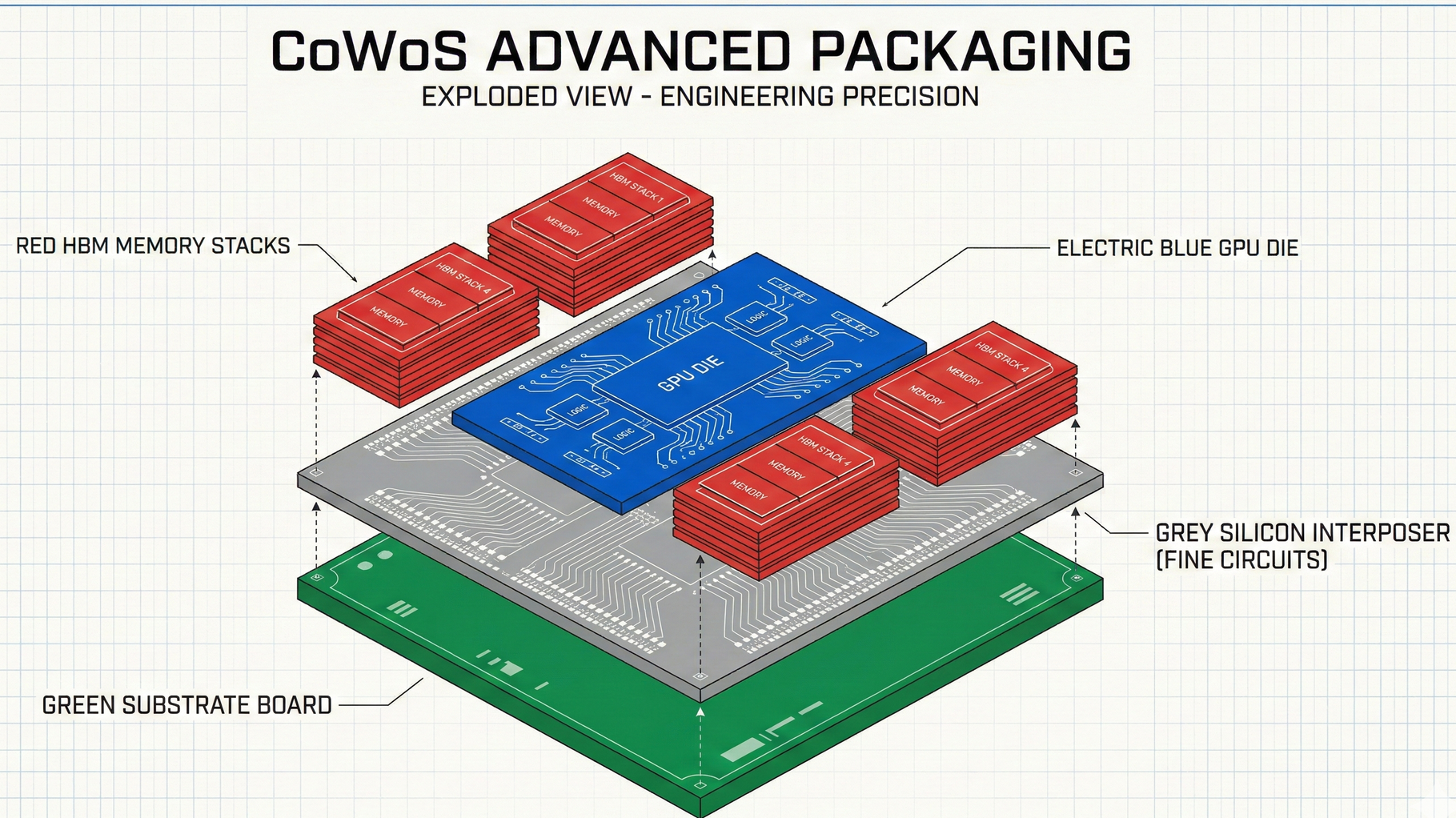
TSMC's monopoly on AI chips is not only because it can manufacture chips, but also because it began strategically deploying CoWoS (Chip-on-Wafer-on-Substrate) as early as 2012.
1. What is CoWoS? Simply put, it involves using a silicon interposer as a "foundation" and tightly stacking GPUs (compute) and HBM (memory) on this foundation.
- Extremely short distance: Electrons travel shorter distances, leading to higher speeds and lower power consumption.
- Extremely high bandwidth: Thousands of wires are embedded in the foundation, allowing GPUs and memory to exchange data at incredible rates.
2. Ten Years to Sharpen a Sword When Morris Chang decided to pursue CoWoS back then, no one was optimistic. It was too expensive, and only FPGA manufacturers were willing to use it. But in the AI era, this "high-bandwidth, low-latency" architecture became an essential requirement. When Intel and Samsung rushed to catch up, they found that TSMC had already filed thousands of packaging patents and possessed a team of engineers who best understood how to "stack LEGO blocks."
4.4 Counterattack from Rivals: The Opportunity of Heterogeneous Integration
This is the only opening for Intel's IDM 2.0 to potentially break through.
- Intel's Foveros/EMIB: Intel is actually very strong in packaging technology (even leading in certain metrics). Its EMIB (Embedded Multi-die Interconnect Bridge) technology does not require an entire expensive silicon interposer; it only needs a "small bridge" at the chip connection points. This is highly competitive in terms of cost. If Intel can convince customers: "It's fine if TSMC makes the chips, but let me handle the packaging," then it can claim a share of the back-end battlefield.
- Samsung's Turnkey: Samsung is promoting a "HBM + Foundry + Packaging" package. For second-tier AI chip manufacturers who cannot secure TSMC's capacity, Samsung's "buy everything from me in one go" service still holds appeal.
Chapter Five: Conclusion — The Age of the Swordsmith
5.1 Final Review of the Three Kingdoms Landscape
1. Intel: This is a story of "imperial revival," but with an uncertain outcome. Intel is painfully attempting to decouple design and manufacturing under the IDM 2.0 architecture. Its future positioning may no longer be that of an absolute hegemon, but rather a "strong U.S. domestic option." Its value is more based on geopolitical security than pure commercial efficiency.
2. Samsung: This is a story of the "resource curse." The money earned from memory allowed it to lose the "wolf spirit" needed for a desperate fight. In the wafer foundry sector, it is difficult for Samsung to shake off the "backup" label. Unless it can leverage the vertical integration of HBM and packaging to find a unique niche in the AI server market.
3. TSMC: This is a victory for the "trust economy." TSMC proved that in a highly complex technology supply chain, "focus" is far more powerful than "all-round capability." Through its Grand Alliance system, it has tied the world's strongest EDA, IP, and design companies to its bandwagon. To defeat TSMC, you cannot defeat just one company; you must defeat the entire semiconductor ecosystem.
5.2 New Era Concerns: Geopolitics and Antitrust
- Silicon Shield: Some say it is Taiwan's protective umbrella.
- Supply Chain Anxiety: Governments in Europe and the U.S. are doing everything they can (subsidies, pressure) to reduce reliance on TSMC and foster Intel or Rapidus.
5.3 Outlook for 2026
Looking at this war from 2026:
- Moore's Law has transformed from a "physical law" into an "economic law" — only the wealthiest (Apple/NVIDIA) can afford the most advanced processes.
- Packaging has become the new Moore's Law.
- Trust remains the most expensive moat.
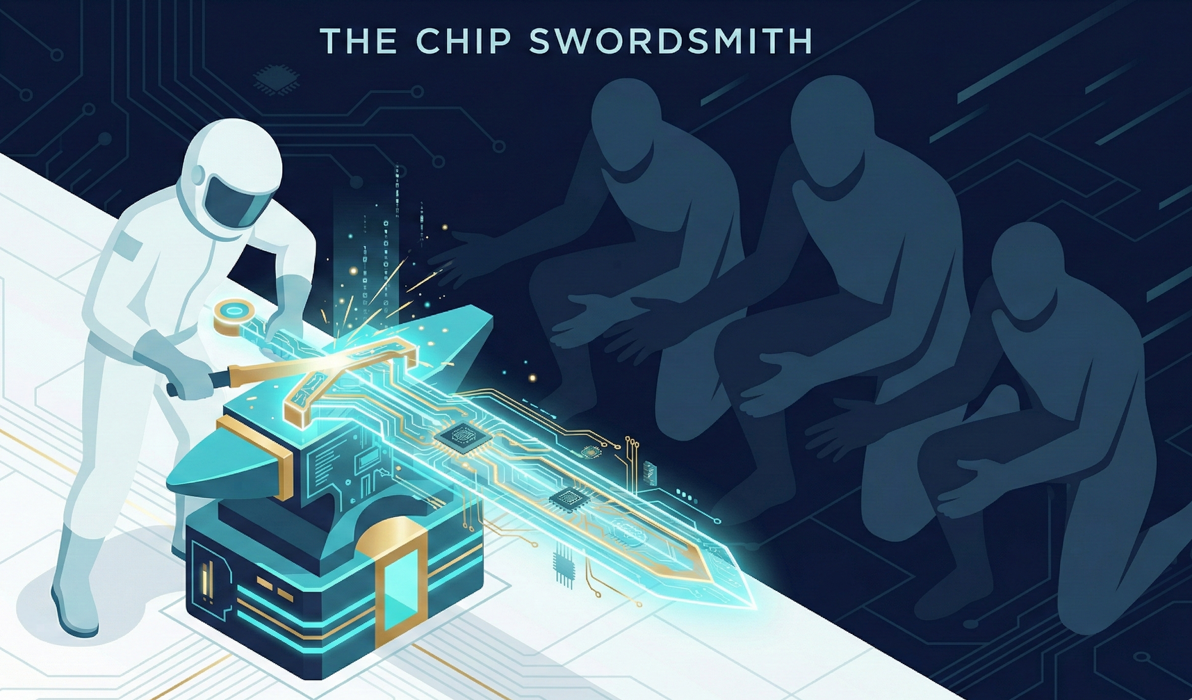
In this golden age of AI explosion, all software companies (OpenAI, Google, Meta) are vying for computing power, and all hardware companies (NVIDIA, AMD) are competing for market share. And behind all this clamor, the "servant" silently wiping down machines and adjusting parameters smiles at it all.
In-Depth Research · Quantitative Perspective
Want more insights from semiconductor quantitative research?
【Insight Subscription Plan】Bid Farewell to Retail Investor Mindset: Build Your Alpha Trading System with "Quantitative Chips" and "Consensus Data"EDGE Semiconductor Research
📍 Series Map — Navigate the Complete EDGE Semiconductor Research →


