Foreword: The Caste System of Silicon Wafers (The Caste System of Silicon)
In stock market forums, we often hear investors ask: "Why is UMC still holding onto 28nm? Isn't that an antique technology from 10 years ago? Does a company like this still have competitive edge?"
This is a huge misconception. In fact, it is precisely these technologies, often regarded as "antiques," that support the operation of modern civilization.
Disassemble a brand new Tesla electric vehicle, and you'll find approximately 2,000 chips inside. Among them, only one or two Full Self-Driving (FSD) computer chips actually utilize TSMC's "advanced process" nodes of 7nm or below; the remaining 99%, controlling functions such as power window operation, power management, Bluetooth connectivity, and air conditioning temperature control, are all manufactured using "mature process" nodes of 28nm, 40nm, or even 90nm.
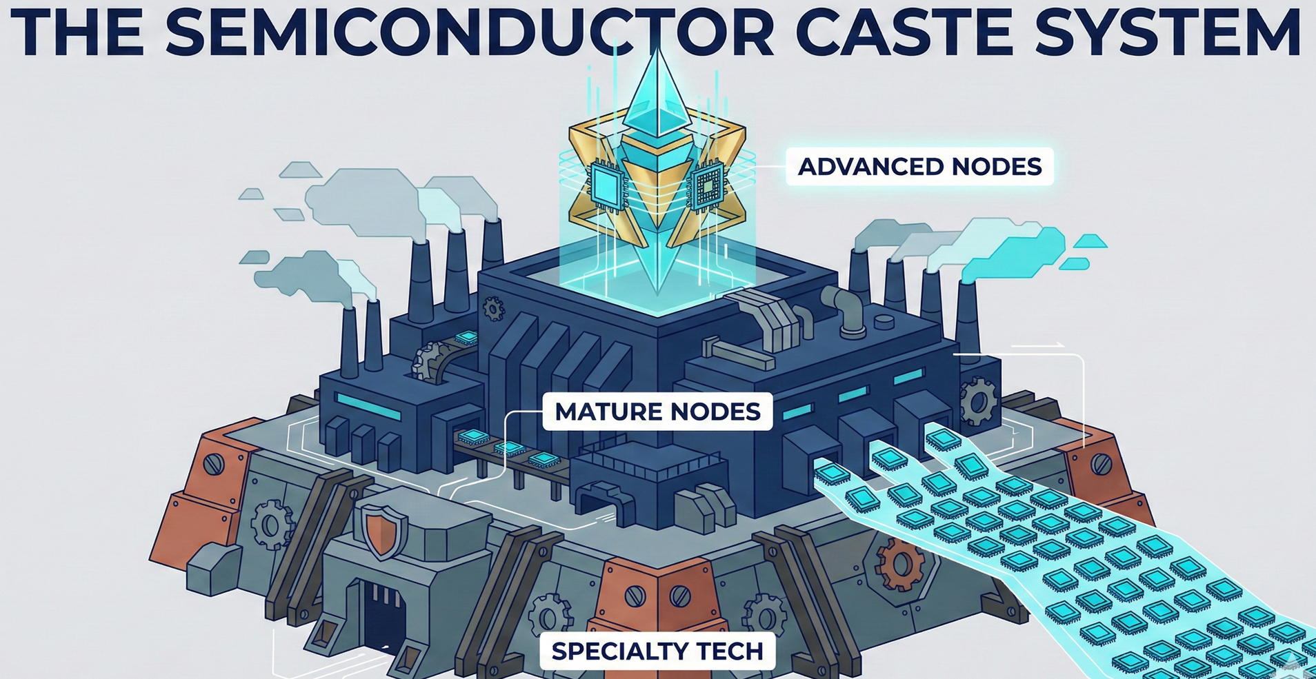
The wafer foundry industry is not a single-dimensional race; rather, it operates like a rigorous "caste system". This system is not based on discrimination, but on a perfect division of labor based on physical properties and commercial benefits.
We categorize the semiconductor manufacturing landscape into three main tiers:
- Advanced Nodes (Advanced Nodes): The nobility challenging physical limits. Serving industries such as AI, High-Performance Computing (HPC), and flagship smartphones.
- Mature Nodes (Mature Nodes): The commoners pursuing depreciation bonuses. Serving industries such as IoT (Internet of Things), automotive controllers, and consumer electronics.
- Specialty Technology (Specialty Technology): The special forces that don't focus on nanometer scales. Serving industries such as high-voltage power, sensors, and optical communication.
Only by understanding this hierarchical structure can you comprehend why TSMC's stock price is viewed through a growth lens, while UMC's is seen through a cyclical lens. Next, we will begin by examining the very top of this pyramid.
Chapter One: Advanced Nodes (Advanced Nodes) —— The Aristocratic Game of Challenging Physics
Scope: 7nm $\rightarrow$ 5nm $\rightarrow$ 3nm $\rightarrow$ 2nm $\rightarrow$ A16 (1.6nm)
Dominant Players: TSMC (dominant leader)、Samsung (struggling to catch up)、Intel (attempting a comeback)
These are the crown jewels of human technology, and a high-stakes gamble where the entry ticket starts in the "tens of billions of US dollars".
In this domain, Moore's Law is no longer a naturally occurring phenomenon, but a physical miracle "forced" into existence by immense capital and brilliant engineers.
1. Revolution in Physical Structure: From Fins to Nanosheets
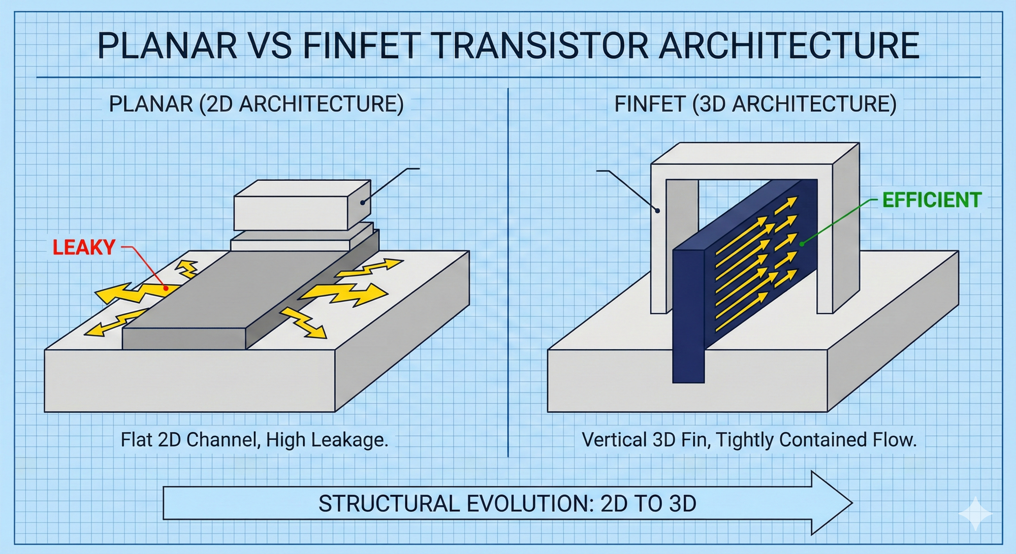
In the process of chip miniaturization, there is only one primary adversary: Leakage.
A transistor operates much like a faucet: the Gate acts as the handle, controlling the flow of current (Source to Drain). When process nodes shrink to a certain extent, this "handle" becomes too short and small to effectively shut off the current, leading to chip heating and power consumption.
1.1 FinFET (Fin Field-Effect Transistor): TSMC's Defining Battle
Prior to 20nm, transistors lay flat on the silicon wafer (Planar). By 16nm, planar gates could only control current from above, akin to trying to press down on a gushing water pipe with just one hand; current would easily leak from the sides.
TSMC introduced FinFET technology at the 16nm node. They "stood up" the conductive channel, shaping it like a fin, and then had the gate envelop the channel tightly from three sides — left, top, and right — like a ㄇ-shaped clamp.
- Result: Increased contact area, stronger control, and the leakage problem resolved.
- Battle: It was this battle that allowed TSMC to decisively pull ahead of Samsung in yield and performance, securing Apple's A-series chip orders with unwavering loyalty ever since.
1.2 GAA (Gate-All-Around): The Holy Grail of 2nm
However, at 3nm and below, even "fins" were no longer sufficient. This is because one side of the fin (the bottom) remained unenclosed, still allowing current to leak.
Thus, humanity invented the ultimate structure: GAA (Gate-All-Around).
- Principle: The fins are laid down and transformed into several suspended "nanosheets," with the gate then enveloping each channel 360 degrees without blind spots, like a donut.
- Current Status: Samsung, in an effort to accelerate, took the risk of introducing GAA (called MBCFET) at 3nm, resulting in disastrously low yields; TSMC, on the other hand, chose a more conservative approach, continuing to use FinFET (squeezing out the last drop of value) at 3nm and only formally introducing GAA at 2nm. This proved to be an extremely wise business decision.
2. The Hegemony of Lithography Machines: EUV and High-NA
If the structure is the foundation, then the lithography machine is the shovel that builds the edifice.
At 7nm and below, traditional DUV (Deep Ultraviolet) can no longer draw such fine lines. This is like trying to draw eyebrows with a thick marker.
2.1 The Capital Wall of EUV (Extreme Ultraviolet)
ASML's EUV machines use a light source with a wavelength of just 13.5 nanometers. This is no ordinary light; it is plasma generated by laser-bombarding tin droplets.
- Price: A single EUV machine costs approximately $150 million to $200 million USD (about NT$5-6 billion). An advanced fab requires at least 10 to 20 such machines.
- Selection Effect: This towering "capital wall" directly blocks second-tier manufacturers from entry. GlobalFoundries and UMC, after calculating the financials, successively announced the cessation of R&D for processes below 7nm, having found the return on investment too low. Since then, advanced process manufacturing has become an exclusive club for TSMC, Samsung, and Intel.
2.2 High-NA EUV: Intel's High-Stakes Bet
To leapfrog competitors in the 2nm realm and beyond, Intel was the first to procure ASML's latest generation High-NA (High Numerical Aperture) EUV machines.
- Cost: A single machine costs upwards of €350 million EUR (approximately NT$12 billion).
- Difference: Its lenses are larger and offer higher resolution, reducing the number of exposures required. TSMC currently remains cautious about it (due to the high cost), planning to leverage existing EUV machines through multi-patterning techniques (Double Patterning) to support production through the A16 process. This reflects a philosophical difference in cost control between the two companies.
3. Business Logic: Death Spiral and the Rich Man's Club
Advanced process nodes are dubbed a "noble's game" not just because manufacturing is expensive, but even more so because "design is expensive".
3.1 The Cost of PPA
Clients pursue advanced process nodes for PPA:
- Power (Power Consumption): More power efficient.
- Performance (Performance): Faster operation.
- Area (Area): More transistors per unit area.
However, this pursuit comes at a cost. Designing a 3nm chip, from acquiring EDA licenses and IP cores to mask fabrication and verification, can incur R&D costs as high as $500 million to $1 billion USD.
This implies that if your chip doesn't sell more than 50 million units, you won't even recoup your R&D expenses.
3.2 Widening Wealth Gap
This has led to a Matthew effect in the IC design industry. Only giants with massive shipping volumes, such as Apple, NVIDIA, AMD, Qualcomm, and MediaTek, can afford to play in the 3nm arena.
Small and medium-sized IC design companies are compelled to remain at 12nm or 28nm. This also explains why TSMC's revenue share from advanced processes is steadily increasing, as it serves some of the wealthiest companies on Earth.
3.3 New Battlefield: Advanced Packaging (CoWoS)
As Moore's Law reaches 2nm, the cost of further physical miniaturization has become prohibitively expensive.
Consequently, the battlefield has shifted to "packaging". TSMC no longer just sells wafers, but 'systems'. Through CoWoS (Chip on Wafer on Substrate) technology, HBM (High Bandwidth Memory) and GPU logic chips are stacked together like building blocks. The current AI chip war is essentially a combination punch of "3nm process + CoWoS packaging". This also explains why Intel, even after spinning off its foundry division, finds it challenging to snatch NVIDIA's orders — because Intel's packaging capacity and yield have yet to catch up.
Chapter Two: Mature Nodes (Mature Nodes) —— The Extremely Profitable Cash Cows and Red Ocean
Scope: 28nm、40nm、55nm、90nm、0.13$\mu$m Dominant Players: TSMC (largest capacity)、UMC (UMC)、GlobalFoundries (GlobalFoundries)、SMIC (SMIC) Keywords: depreciation bonus、long-tail effect、Red Supply Chain
Here, the rules of the game completely change. It's no longer about pursuing "speed," but about pursuing "stability" and "affordability". This is a massive market that appears calm but is actually rife with undercurrents (a "red tsunami").
1. Sweet Spot (Sweet Spot): Why will 28nm never die?
In the history of semiconductors, 28nm is a legendary "long-lived node". According to Moore's Law, older process nodes should eventually be phased out, but 28nm has not only survived but its demand is actually growing. Why?
1.1 The Golden Cross of Physics and Economics
- Physical Limit: 28nm represents the pinnacle of Planar FET (Planar Field-Effect Transistor). Moving further down (22nm/16nm) necessitates the introduction of a three-dimensional FinFET structure.
- Cost Cliff: While FinFET offers superior performance, its mask costs and manufacturing expenses surge dramatically. For chips that don't require extreme computing power, using FinFET is overkill.
- Conclusion: 28nm has become the node with the "lowest unit cost" and the "highest cost-performance ratio". It is the Toyota Altis of the semiconductor world — not the fastest, but the most economical, practical, and durable.
1.2 The Cornerstone of the Internet of Things
Who resides at 28/40nm?
- Wi-Fi 6/7 Chips: Routers don't need to run AI models; they just need to transmit data reliably.
- OLED Driver IC (DDI): Chips that control screen brightness.
- ISP (Image Signal Processor): Chips that process camera images.
- IoT MCU: Smart speakers, air conditioning controllers, automotive central displays.
As long as humans need to connect to the internet and view screens, the demand for 28nm will always exist.
2. Financial Magic: Depreciation Bonus (Depreciation Bonus)
Investors often ask: "UMC isn't building 3nm fabs, so where's its future growth?" The answer lies in the financial statement structure. The core business model for mature process foundries is to operate like a "landlord who has paid off the mortgage".
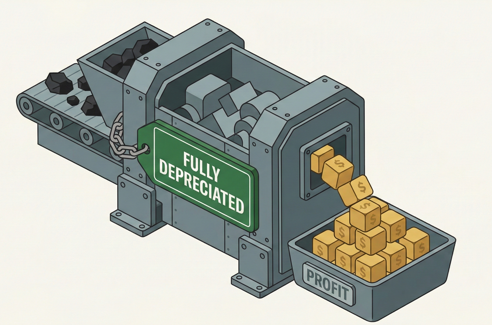
2.1 The Five-Year Deadline
Building a wafer fab costs billions of dollars, and for the first 5 to 7 years, these equipment incur massive "depreciation expenses" reported annually in financial statements. During this period, the fab operates primarily to pay off debt.
- Turning Point: After 5 years, the equipment's depreciation is fully accounted for.
- High-Profit Mode: At this point, even though the lithography machine is older, it can still print perfect 28nm chips. The revenue from selling chips, after deducting utilities, materials, and labor, is almost entirely pure profit.
2.2 UMC's Elegant Transformation
In 2018, UMC announced its decision to abandon R&D for advanced processes below 12nm. The market was in an uproar at the time, viewing it as a surrender. It turned out to be the wisest decision in UMC's history.
- Avoiding the Meat Grinder: UMC avoided direct confrontation with TSMC and Samsung in the capital-intensive EUV arms race.
- Focus on ROI: They focused on optimizing specialty processes at 22/28nm, capitalizing on depreciation bonuses. Their gross margin surged from 15% to 30%-40%, transforming them into a stable, high-dividend stock.
3. The Red Threat: SMIC and the "Mature Process Tsunami"
However, this cozy haven is now facing its biggest challenge ever.
3.1 Forced Capacity Build-up
As the US blocked access to EUV and equipment for processes below 14nm, China (SMIC, Hua Hong Semiconductor) was compelled to pour hundreds of billions in state subsidies entirely into 28nm and more mature processes.
- Strategy: Since we cannot produce the most advanced CPUs, we will take over the global market for home appliances, automotive, and industrial control chips.
- Current Situation: According to statistics, China accounts for over 60% of the world's newly added capacity in mature processes. This signifies that a fierce price war is imminent.
3.2 Two Worlds of Supply Chains
This will lead to the commoditization and fragmentation of the mature process market.
- Red Ocean for Standard Products: Generic chips like USB controllers will face a price war from Chinese manufacturers.
- De-Americanization vs. De-Sinicization: European and American automakers (e.g., Ford, GM), driven by national security and supply chain resilience concerns, may demand "non-Red supply chains" (i.e., chips not manufactured in China). This will be the future moat for UMC, PSMC, and VIS — earning a "geopolitical premium".
Chapter Three: Specialty Technology (Specialty Technology) —— The Invisible Special Forces
Scope: Not focused on nanometer scales, but on "physical functions" (More than Moore) Dominant Players: TSMC、Vanguard (Vanguard International Semiconductor)、Tower Semi (Tower Semiconductor)、STM (STMicroelectronics) Keywords: BCD、High Voltage、MEMS、Compound Semiconductors
While everyone else is striving for "how thin the linewidth must be" (nanometer scale), there's a group saying, "I don't make it small; I make it robust." Specialty technology doesn't pursue the miniaturization dictated by Moore's Law, but rather aims for the ultimate physical characteristics. This embodies the "artisan spirit" in the semiconductor industry.
1. BCD and High-Voltage Processes: The Power Tamer
Applications: Power Management ICs (PMIC)、EV inverters、fast chargers.
1.1 Delicate vs. Robust
Advanced 3nm transistors are very delicate, typically operating at just 0.7V. If you directly inject a 400V electric vehicle battery voltage into it, the chip would instantly vaporize. Handling high voltages requires completely different manufacturing processes.
1.2 BCD Process (Bipolar-CMOS-DMOS)
This is a "black technology" that integrates three different types of transistors onto a single chip:
- Bipolar (Bipolar): Handles analog signals with high precision.
- CMOS (Complementary Metal-Oxide-Semiconductor): Processes digital logic, responsible for computations (the "brain").
- DMOS (Double-Diffused Metal-Oxide Semiconductor): Power components, robust and capable of handling high voltage and large currents (the "muscles").
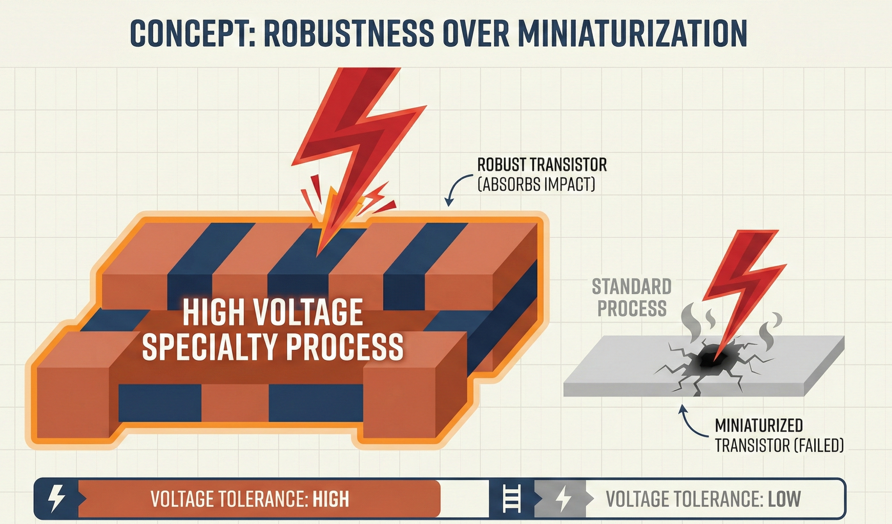
Vanguard International Semiconductor (VIS) is a leader in this field. They don't need to purchase EUV machines but rather focus on making DMOS more robust against voltage and better at heat dissipation. This is also why, as electric vehicles become more widespread, specialty processes become more profitable.
2. MEMS (Micro-Electro-Mechanical Systems): Micro-Sculptures on Silicon Wafers
Applications: Mobile phone microphones, accelerometers (screen rotation detection), pressure sensors.
This isn't about "drawing circuits" on a planar surface, but about "building mechanical structures" on silicon wafers.
- Micro-Sculpting: Engineers use etching techniques to carve micron-scale cantilevers, membranes, and springs onto silicon wafers.
- Principle: When you speak, sound waves vibrate the tiny silicon membrane, causing a change in capacitance that is converted into a digital signal. This requires extremely precise mechanical control capabilities, completely different from traditional logic processes, and has a very high technological barrier.
3. Compound Semiconductors: The Rise of the Third Generation (SiC / GaN)
This falls under the broader category of specialty processes and is currently one of the hottest "battlegrounds".
- SiC (Silicon Carbide): Resistant to high temperatures and high voltages. It is the core material for Tesla's inverters.
- GaN (Gallium Nitride): Fast switching speed. It is the secret behind the small, high-wattage "fast chargers" you hold in your hand.
While TSMC is unrivaled in the silicon-based domain, the manufacturing process for compound semiconductors involves specialized epitaxy technology. This is an entirely new arena, and TSMC is actively strategizing, attempting to leverage its scale advantage from silicon-based manufacturing for a "dimension-reduction strike".
Conclusion: The Panoramic Map of Wafer Foundries —— An Investor's Survival Guide
Dear reader, after reviewing these three chapters, the semiconductor landscape should now be clear in your mind. Chips are more than just "high-tech"; they are a clearly defined, organic ecosystem.
1. Ecosystem Symbiosis
Imagine an AI server:
- Its brain (NVIDIA H100) must use TSMC's 4nm (Advanced Process).
- Its memory controllers and network cards might use 28nm (Mature Process).
- Its power supply must use BCD High-Voltage Process (Specialty Technology).
Each is indispensable. Advanced processes determine the upper limits, but mature and specialty processes define the baseline and stability.
2. Strategic Summary Table
| Process Tier | Representative Process | Key Equipment | Business Model | Moat | Investment Keywords |
|---|---|---|---|---|---|
| Advanced Process | < 7nm (GAA/FinFET) | EUV (ASML) | Arms race. High capital expenditure, oligopolistic market. | Physical limits, capital barrier | Growth, AI, technological leadership (TSMC) |
| Mature Process | 28nm - 90nm | DUV | Cash cow. Depreciation complete, compete on cost and yield. | Capacity scale, depreciation bonus | Dividend yield, cyclicality (UMC) |
| Specialty Technology | BCD, MEMS, HV | Specialized equipment | Customization. Focus on functionality, not size; low volume, high variety. | Physical characteristics (high voltage resistance/sensing) | Niche market, stable gross margin (Vanguard) |
This is the caste system of chips. Within this system, there is no such thing as "backward" technology; there is only technology placed in the wrong position. Understanding this point means understanding the true operational logic of the semiconductor industry.
In-Depth Research · Quantitative Perspective
Want more quantitative research insights on semiconductors?
【Insight Subscription Plan】Break Free from Retail Investor Mindset: Build Your Alpha Trading System with 'Quantitative Flows' and 'Consensus Data'EDGE Semiconductor Research
📍 Series Map — Navigate the Complete EDGE Semiconductor Research →


