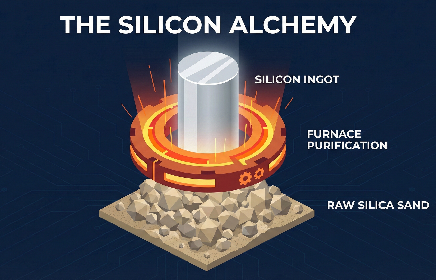
Introduction: The Ultimate Purity on Earth (The Quest for 11N)
The first step in semiconductor manufacturing does not take place in the yellow light area of a cleanroom, but by a furnace operating at temperatures exceeding 1400°C. This is a modern alchemy. The mission is simple, yet seemingly impossible: to refine common roadside sand (silicon dioxide) into monocrystalline silicon with a purity of 99.999999999%.
This is known in the industry as "11N" (eleven nines). To help you understand just how extreme this purity is, let's make a comparison:
- Gold (99.99%): This is what we commonly refer to as 4N pure gold.
- Silicon Wafer (11N): This is equivalent to "not finding a single person with a cold among the entire 8 billion people on Earth."
Why such extreme purity? Because in TSMC's 3-nanometer process, the gate width of a transistor is only a few dozen atoms wide. If even one impurity atom (such as oxygen or carbon) is present, current will leak when it shouldn't, or be blocked when it should flow. An NVIDIA B200 chip produced from such a wafer would be directly scrapped, and tens of thousands of dollars would instantly evaporate.
This is the value of silicon wafer manufacturers (such as Shin-Etsu and GlobalWafers). They do not sell material; they sell "ultimate order and purity."
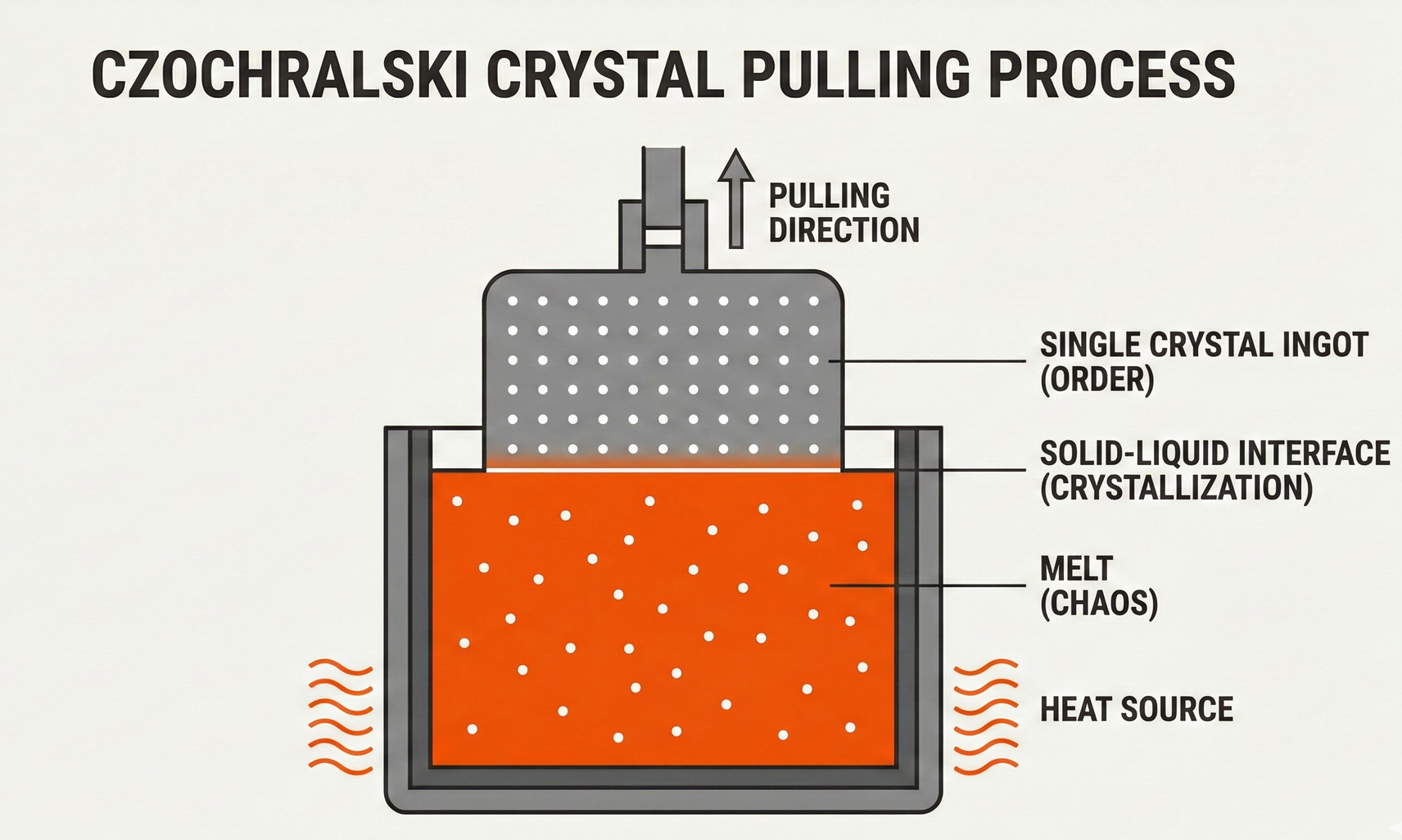
Chapter 1: Crystal Pulling — Pulling a Perfect "Silver Radish"
"All high-tech chips are initially 'grown' from a pot of glowing magma. This is a process that defies the thermodynamic law of entropy increase, where we force atoms from chaos towards absolute order."
To make a wafer, one must first produce a crystal ingot. This is a physical transformation process, and the industry uses the Czochralski process (CZ method).
1.1 Fishing in Hell: CZ Method Crystal Growth
Imagine a massive quartz crucible filled with Electronic Grade Silicon (EGS)—these are high-purity silicon chunks that have already been refined, resembling a pile of broken grey stones.
1. Melting Heaters boost the temperature above 1400°C. The silicon chunks melt into a golden-yellow, glowing liquid magma. At this point, all silicon atoms are wildly darting around (Brownian motion).
2. The Allure of the Seed Crystal Engineers lower a thin wire from above, with a pencil-sized monocrystalline silicon rod tied to its end. This is called a "seed crystal." Its internal atomic arrangement is perfect. When the seed crystal gently touches the surface of the liquid magma, a miracle occurs. The liquid silicon atoms, "attracted" by the perfect atomic arrangement of the seed crystal's surface, begin to obediently align themselves one by one according to the seed crystal's pattern (lattice direction), cooling and solidifying.
3. Rotation and Pulling This is the most difficult step. The machine rotates the seed crystal while very slowly pulling it upwards at a speed of only a few millimeters per hour.
- Pull too fast: The crystal ingot will become too thin, or even break.
- Pull too slow: The crystal ingot will become too thick, leading to defects. This is like pulling taffy, but this "taffy" has a diameter of 30 centimeters (12 inches) and weighs hundreds of kilograms. To suspend this enormous "silver radish" in mid-air, maintaining absolute verticality and stable rotation, requires extreme mechanical control.
1.2 Military Parade Formation vs. New Year's Eve Crowd: The Difference Between Monocrystalline and Polycrystalline
Why must chips be made using this expensive CZ method to pull monocrystalline silicon? Can't we simply pour silicon melt into a mold and cool it into polycrystalline silicon, like making ice cubes?
We can use this analogy:
- Polysilicon — "New Year's Eve Crowd"
- Structure: Like a subway station on New Year's Eve, although everyone is a person (silicon atom), some groups walk east, others walk west.
- Defect: The interface where crowds meet is called a "grain boundary."
- Consequence: When current (electrons) flows through, it collides with these chaotic groups, leading to slower speeds and generating high heat.
- Application: This quality is only suitable for solar panels (where electricity generation is the goal, not speed).
- Monocrystalline Silicon — "Military Parade Formation"
- Structure: Like a North Korean military parade. Hundreds of millions of atoms, all facing the same direction, with identical spacing and perfectly uniform formation.
- Advantage: There are no "grain boundaries" internally. Electrons flow through like speeding on an open highway, unhindered.
- Application: This is the only choice for making CPUs, GPUs, and memory.
1.3 The Geometrically Increasing Difficulty of 12-inch Wafers
This is also why 12-inch wafers (300mm) are currently the mainstream, and why it is difficult to further develop 18-inch (450mm) wafers. The thicker and heavier this "radish" becomes, the more severe the interference from gravity, surface tension, and thermal convection during the pulling process. Currently, the number of manufacturers worldwide capable of consistently pulling perfect 12-inch monocrystalline ingots can be counted on one hand (Shin-Etsu, SUMCO, GlobalWafers). This is not something that can be achieved simply by purchasing machinery; it is the result of decades of accumulated "parametric black magic."
Chapter 2: Slicing and Processing — Nanometer-level Flatness
"If you were to magnify a 12-inch wafer to the size of Earth, the height difference on its surface (between the highest peak and the deepest trench) could not exceed 3 centimeters. This is the semiconductor industry's definition of 'flatness'."
The freshly pulled crystal ingot has tapered ends and a rough surface. To transform it into mirror-smooth wafers, it must undergo three critical processes.
2.1 Violent Gentleness: Diamond Wire Sawing
First, this 2-meter long, hundreds-of-kilograms heavy silicon ingot must be sliced into thin slices, each with a thickness of only about 0.775 millimeters (mm).
1. Like slicing ham, but harder In earlier times, inner-diameter saws were used. Now, the mainstream method is Diamond Wire Sawing. This involves a high-strength steel wire coated with diamond micro-powder, pulled back and forth across the ingot at extremely high speeds.
- Challenge: This wire must be stretched extremely taut, and the cutting path must not have any warp or bow. Even a slight deviation will result in uneven wafer thickness, which cannot be corrected later.
- Kerf Loss: The slicing process itself grinds away some silicon (turning it into silicon powder). This is like sawdust generated when sawing wood. For expensive monocrystalline silicon, these losses represent money. Manufacturers with superior technology (such as GlobalWafers) achieve narrower kerfs and less loss, thus higher gross margins.
2. Edge Grinding The edges of freshly sliced wafers are extremely sharp, like blades. If struck during transport, the edges can chip, and the resulting micro-dust can contaminate the entire cleanroom. Therefore, special grinding wheels must be used to round off the wafer edges. This is like filing freshly clipped fingernails.
2.2 The Globe Metaphor: CMP Polishing
Although a sliced wafer appears flat to the naked eye, under a microscope, its surface is cratered like the moon. At this point, CMP (Chemical Mechanical Planarization) is required.
1. Physical Standard: DOF (Depth of Focus) Why such extreme flatness? Because ASML's EUV lithography machines use extremely short wavelengths of light, resulting in a very shallow Depth of Focus (DOF).
- Analogy: It's like taking a photo with a wide-aperture lens, where the focal range is very narrow.
- Consequence: If the wafer surface has even slight height variations (e.g., a difference of just a few dozen nanometers), the circuit pattern will be "out of focus" and blurred.
2. Extreme Flatness After coarse grinding, etching, and polishing, the final wafer surface flatness must be at an atomic level. There is a famous industry analogy: "If a 12-inch wafer were magnified to the size of Earth, the height difference between the highest peak and the deepest trench on its surface could not exceed 3 centimeters." This exemplifies the extreme craftsmanship of silicon wafer manufacturers.
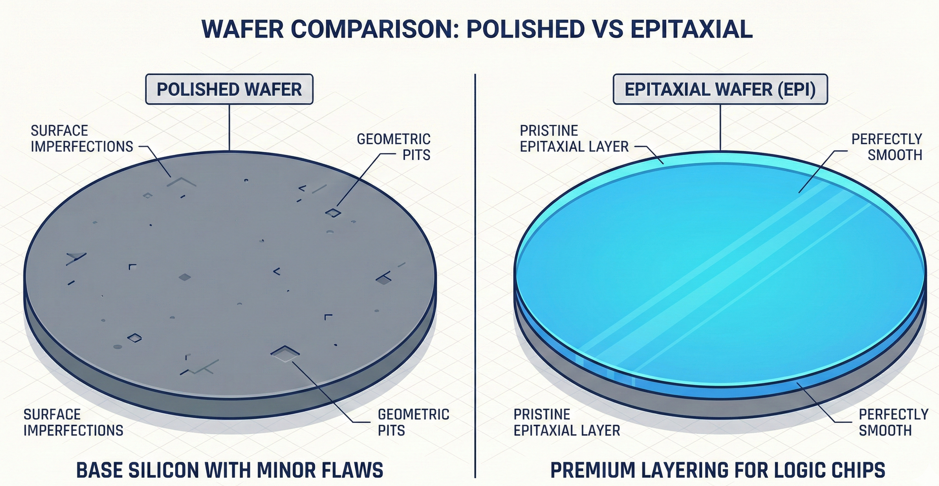
Chapter 3: Epitaxy (Epi Wafer) — The Exclusive Floor of the Aristocracy
"In the world of wafers, the hierarchy is strict. Some wafers are born to reside in the crowded dormitories of memory, while others are destined to become the marble floors of a CPU palace."
For investing in the silicon wafer industry, this is the most crucial chapter. Because wafers are categorized into two types: Polished Wafers (PW) and Epitaxial Wafers (Epi). This distinction determines a company's gross margin and strategic position.
3.1 Polished Wafer: Ordinary Tiles
Definition: These are wafers that have completed the processes described in Chapter 2, undergoing slicing and polishing. Application: Primarily used for DRAM (Dynamic Random-Access Memory) and NAND Flash (flash memory).
Why can memory chips use ordinary "flooring"? Because the structure of memory (such as 3D NAND) is like building a skyscraper, stacking layers one by one. The underlying silicon wafer primarily serves as the "foundation." While flatness is required, the tolerance for extremely small crystal defects on the surface is relatively higher. Commercial Characteristics: High volume, but intense price competition, making them a "cash cow" for silicon wafer manufacturers.
3.2 Epitaxial Wafer (Epi Wafer): Italian Marble
Pain Point: COP Defects No matter how good the polishing technology is, physical grinding will always cause tiny damage to silicon atoms or leave behind microscopic voids (COP) from the original crystal growth. For logic integrated circuits (Logic ICs)—such as TSMC's 3nm CPUs and NVIDIA's GPUs—these minute defects are fatal. Because the circuits of logic chips are laid flat on the "floor," if there is an atomic-level pit on the floor, electrons will get stuck, leading to computational errors.
Solution: Adding Another Layer (Epitaxy) Therefore, silicon wafer manufacturers perform an expensive process on top of polished wafers: epitaxy.
- Process: Using CVD (Chemical Vapor Deposition) technology, gaseous silicon atoms are deposited layer by layer onto the wafer surface at high temperatures.
- Result: A brand-new, atomically perfectly arranged layer of pure silicon is grown.
- Analogy: It's like finding the original cement floor inadequate and spending a fortune to lay a layer of the highest-grade seamless marble on top.
Strategic Significance:
- TSMC's Essential Need: All logic chips for advanced processes (7nm/5nm/3nm) must use Epi Wafers 100% of the time.
- Profit King: Epi Wafers are 30% to 50% more expensive than polished wafers, and the technological barrier is extremely high. Whoever can produce the best Epi wafers secures TSMC's orders.
Chapter 4: The Imperial Landscape of Silicon Wafers
"The hegemon of wafer foundry is in Taiwan, but the hegemon of wafer materials is in Japan. This is an extremely closed, highly oligopolistic market, where the top five manufacturers control 90% of global capacity. This is Japan's last semiconductor stronghold, and their strongest bargaining chip."
4.1 Japan's Backyard Garden: Shin-Etsu & SUMCO
A characteristic of the silicon wafer industry is that "the strong get stronger." Because the parameter tuning of crystal pulling furnaces is the accumulation of decades of experience (the so-called "know-how"), new entrants can hardly cross the yield rate chasm.
This market is guarded by two Japanese giants, whose combined market share exceeds 50%.
1. Shin-Etsu Chemical: God of Semiconductor Materials
- Status: World No. 1.
- Moat: Shin-Etsu not only produces silicon wafers but also monopolizes countless critical materials in semiconductor manufacturing processes, such as photoresists and EUV pods.
- Strategic Significance: It holds the "recipe" for going from 0 to 1. When TSMC develops 2-nanometer processes, Shin-Etsu's scientists must be invited to jointly develop wafers and photoresists compatible with the new process. This is a symbiotic relationship.
2. SUMCO: The Technical Gem of Conglomerates
- Background: Formed by the merger of Mitsubishi Materials and Sumitomo Metal.
- Features: Possesses extremely deep technological expertise, focusing on high-end logic and memory wafers. It is a core supplier to TSMC and Intel.
4.2 Pride of Taiwan: GlobalWafers (6488)
Amidst the dominance of Japanese players, Taiwan's GlobalWafers carved out its own path and firmly established itself as the world's third-largest.
This success is attributed to two major strategic innovations by Chairman Doris Hsu, known as the "Wafer Queen."
1. Growth Through Mergers & Acquisitions (M&A Strategy)
Japanese companies are conservative and do not favor aggressive capacity expansion. GlobalWafers, on the other hand, adopted an aggressive M&A approach.
- Achievements: Acquired US-based SunEdison and Denmark-based Topsil. Although the acquisition of Germany's Siltronic was hindered by geopolitical factors, its ambition for capacity expansion has never ceased. This allowed GlobalWafers to rapidly acquire factories and technological patents worldwide.
2. Long Term Agreement (LTA) Model
This is GlobalWafers' greatest contribution to the industry's business model.
- Past: Silicon wafer prices fluctuated wildly with business cycles.
- Present: Doris Hsu implemented a "sign contracts first, then build factories" approach.
- Negotiation Logic: "TSMC, Samsung, you want me to expand 12-inch wafer capacity? Yes, but first, sign a 5-year guaranteed purchase agreement (LTA) and make an upfront payment."
- Result: This transformed GlobalWafers' financial reports from that of a "cyclical stock" into a stable "bond-like stock." Holding advance payments totaling hundreds of billions of New Taiwan Dollars allows it to weather the semiconductor downturn.
📊 Strategic Summary: The Battlefield Canvas
This is the complete picture of the silicon wafer industry. We can summarize the commercial value of this "silver radish" in a table:
| Wafer Type (Type) | Core Process (Process) | Application (Application) | Price (Price) | Strategic Value (Strategic Value) |
|---|---|---|---|---|
| Polished Wafer (Polished Wafer) |
Slicing $\rightarrow$ Grinding $\rightarrow$ Polishing | DRAM, NAND Flash (Memory) |
Ordinary | Cash Cow Bulk demand from memory manufacturers, highest volume, but more intense competition. |
| Epitaxial Wafer (Epi Wafer) |
Polishing $\rightarrow$ New Layer Growth (CVD) | CPU, GPU, AI Chips (Logic Computing) | Expensive (+30~50%) |
Strategic Stronghold Essential need for TSMC's advanced processes. Highest technical barrier, fattest profits. |
| SOI Wafer (SOI Wafer) |
Insulating layer in the middle (Buried Oxide) | 5G RF, Automotive High-Voltage (Specialized Applications) |
Extremely Expensive | Niche Monopoly Dominated by Soitec (French company). Specializes in handling high-frequency and high-voltage signals. |
Chapter 5: Conclusion — The Silent Cornerstone
"If TSMC is the 'heart' of the semiconductor world, then silicon wafer manufacturers are the 'bone marrow' responsible for generating blood. Without this 11N pure silver radish, NVIDIA's B200 blueprints would remain mere 0s and 1s in a computer, never becoming reality."
In this report, we have observed the intertwining of extreme craftsmanship and geopolitical strategy.
- Physical Extremity: From crystal pulling at 1400°C, to globe-like polishing, and then to atomic-level epitaxy. This is industrial civilization's highest tribute to "purity" and "flatness."
- Business Acumen: GlobalWafers successfully transferred the risk of high capital expenditure to downstream customers through its LTA long-term contract model, creating stable cash flow.
- Geopolitical Balance: We often say that Taiwan controls chip manufacturing (Fab), but let's not forget that Japan controls chip materials (Material).
Investment Implications:
As the AI wave drives TSMC's aggressive expansion of 3nm and 2nm production, remember to look upstream.
Every expensive AI chip produced by TSMC is underpinned by an Epi Wafer from Shin-Etsu, SUMCO, or GlobalWafers.
This is a battle that requires not just technology, but also "recipes" and "scale."
Deep Research · Quantitative Perspective
Want more insights from semiconductor quantitative research?
【Insight Subscription Plan】Break Free from Retail Investor Mindset: Build Your Alpha Trading System with "Quantitative Chips" and "Consensus Data"EDGE Semiconductor Research
📍 Series Map — Navigate the Complete EDGE Semiconductor Research →


