Foreword: Please Temporarily Forget Physics
Before we truly delve into the most profound and expensive world of semiconductor "photolithography," I want you to do one thing: temporarily cast aside all those physics terms that make your head hurt—diffraction, wavelength, refractive index, standing wave effect.
Because once we get bogged down in those details, it's easy to lose sight of the core purpose of this entire process.
In fact, the fundamental principle of chip manufacturing is logically identical to the "cardboard spray painting" we played with as children in the park, or the "hand shadow game" we played with a flashlight. The only difference is that this game in a wafer fab takes place at the nanoscale, and the "spray gun" is worth one hundred million US dollars.
In this chapter, we will use the simplest intuition to deconstruct one of the most precise crafts in human history. Understanding this article will allow you to easily grasp the subsequent in-depth articles on optics and chemistry.
Chapter 1: Core Logic – What Exactly Are We Doing?
Imagine an extreme challenge: you must draw a perfect Pikachu on a wall.
But there's a strict limitation: this Pikachu is only the size of a bacterium, and you cannot draw it directly with a pen.
Why can't you draw it directly?
- Shaky hands: In the nanoscale world, human hands are as massive and clumsy as Godzilla.
- Too slow: A single chip has tens of billions of transistors. If you were to draw them one by one, it would take ten thousand years to finish one chip.
Engineers' Solution: Stenciling
Since we can't draw, we'll "stamp" it.
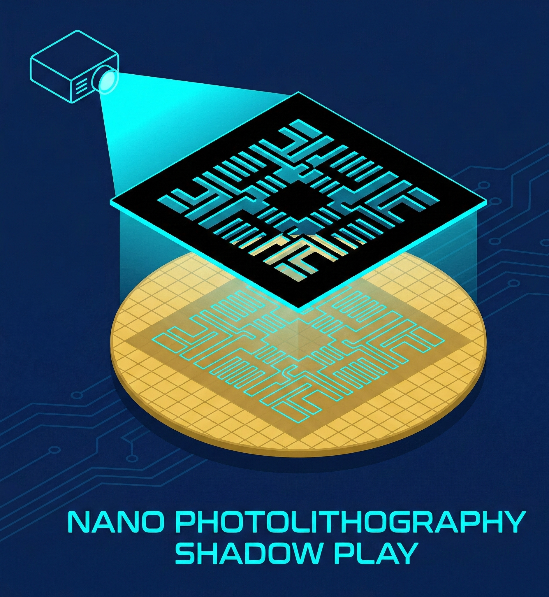
The essence of photolithography is to massively and rapidly transfer complex circuit diagrams (blueprints) designed on a computer onto silicon wafers (the canvas) using light.
To achieve this, we need three core elements. It is crucial to remember their correspondences:
- Photomask (Mask) $\rightarrow$ Your "Template"This is like a stencil plate used for spray painting, or a transparency film.
- Its role: It is pre-etched with the circuit pattern. The black areas block light, and the transparent areas allow light to pass through.
- Photoresist $\rightarrow$ Your "Magic Canvas"This is the most crucial magic in photolithography. It's not ordinary paint, but a layer of highly light-sensitive "glue."
- Its role: Areas exposed to light will change their properties (become softer or harder), while areas not exposed to light remain unchanged. It records the traces left by light.
- Light source $\rightarrow$ Your "Spray Gun"Light passes through the template, hits the glue, completing the pattern transfer.
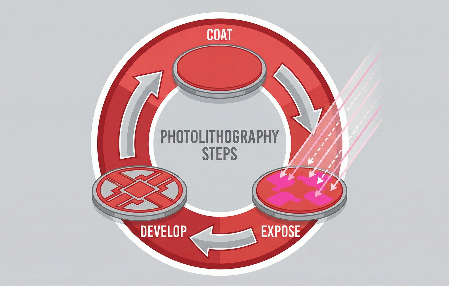
Chapter 2: Three Steps — The Standard Procedure for Pattern Replication
Regardless of whether the chip is 7 nanometer or 28 nanometer, and regardless of whether the machine is ASML's EUV or Nikon's older equipment, photolithography always involves these three steps in a continuous cycle.
Imagine this sequence of actions: apply glue $\rightarrow$ expose to light $\rightarrow$ rinse.
Step One: Coating — Applying the Photosensitive Layer
We cannot engrave directly onto silicon wafers because silicon wafers are too hard, and we don't have knives small enough.
Therefore, the first step is to uniformly apply a thin layer of "photoresist liquid" onto the wafer surface.
- Action: Like making a crepe, the photoresist is dropped onto the center of the wafer, which is then spun at high speed to spread the liquid evenly.
- Plain language translation: We are covering the wall (wafer) with a layer of "photosensitive stickers." This layer of stickers is currently blank, awaiting information to be written.
Step Two: Exposure — The Hand Shadow Game
This is the most critical step, and the moment when the photolithography machine (scanner) demonstrates its power. We use intense light passing through the "photomask (template)" to illuminate the freshly coated wafer.
- Action: Light passes through the openings on the template, is reduced in size by lenses during this process (like a shrinking ray), and finally hits the "photosensitive stickers" on the wafer.
- Miraculous change (invisible ink): If you look at the wafer at this point, you'll find that nothing appears to have changed. However, the chemical properties of the sticker areas exposed to light have already transformed (in mainstream processes, they become easily soluble).
- This is like the "invisible ink letters" we wrote as children; the words are already there, but invisible to the eye. In technical terms, this is called a "Latent Image."
Step Three: Development — The Truth Revealed
Finally, the wafer is sent for "rinsing" and sprayed with a developer solution.
- Action: Chemical agents selectively dissolve the "softened" parts.
- Plain language translation: The sticker areas that were "exposed to light" are thoroughly washed away by the solution, revealing the underlying silicon wafer. Meanwhile, the areas not exposed to light (i.e., the black parts on the photomask) remain stubbornly intact.
- Result: Now, the wafer has a "three-dimensional sticker protective layer" identical to the photomask pattern.
- Note: We haven't etched the circuits into the wafer yet! We have only created shapes using the photoresist (stickers).
Chapter 3: Why Is This So Difficult?
It sounds simple, right? Apply glue, expose to light, rinse. So why do photolithography machines cost hundreds of millions of US dollars? Why is 7-nanometer so difficult to produce?
There's only one answer: because the lines we need to draw are incredibly fine.
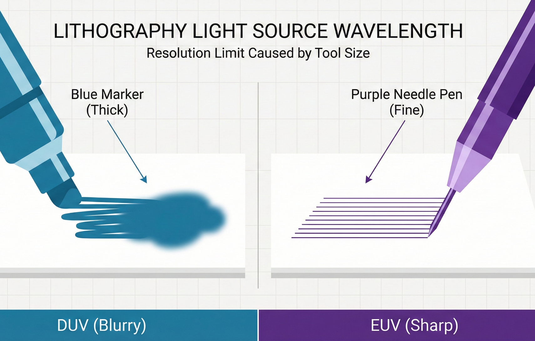
1. The Problem of a Pen Tip That's Too Thick (Light Source Wavelength)
Try to imagine being given a thick-tipped marker and being asked to copy the Heart Sutra onto a grain of rice without the characters blurring together. That's an impossible task, right?
In the world of photolithography, the light source is that pen.
- The "wavelength" of light determines the "thickness of this pen's tip."
- If the light wavelength we use is too long (the pen tip is too thick), when we try to draw two very close lines, these two lines will "blur together" into a large inkblot.
This is why TSMC and Samsung are constantly pursuing shorter-wavelength light sources:
- DUV (Deep Ultraviolet): Like a ballpoint pen, it can be used to draw thicker lines.
- EUV (Extreme Ultraviolet): Like the finest needle-tip pen. Its wavelength is only one-tenth that of DUV, allowing us to draw clear lines in much smaller spaces.
- This is related to "Rayleigh criterion" and "diffraction limit" which will be mentioned in article 2-2-1.
2. The Problem of Shaky Hands (Alignment and Stability)
At the nanoscale, even the slightest vibration is a disaster.
- If the photolithography machine shakes slightly (even by a few nanometers), it's like your hand trembling while applying eyeliner, and the entire wafer is ruined.
- Moreover, we don't just draw one layer. A chip is like a building, with 60 to 80 layers. Each layer must be perfectly aligned with the previous one. This is like stacking 80 coins; if just one is misaligned in the middle, the entire tower collapses.
Chapter 4: The Stickers Are Applied, What Next?
Many people mistakenly believe that once photolithography is complete, the circuits are finished. Wrong!
Remember this crucial statement:
The purpose of photolithography is merely to create a layer of "masking tape."
That layer of photoresist (patterned stickers) left after development is not conductive itself; it is not the circuit. It is a "sacrificial layer" that exists to protect the underlying wafer.
Next, the real main event begins:
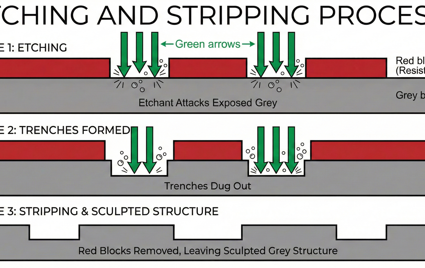
Step Four: Etching — The Real Engraving
Now there are two regions on the wafer:
- Areas protected by stickers: Safe.
- Areas without stickers (where development washed them away): Exposed silicon wafer.
At this point, we take the entire wafer and spray it with strong acid or bombard it with plasma (this is called etching).
- Result: The exposed silicon wafer is corroded, creating a deep trench. The silicon wafer underneath the sticker-protected areas remains intact.
Step Five: Stripping — Mission Accomplished, Then Retreat
After etching is complete, that hardworking "photoresist sticker" has fulfilled its historical mission.
We remove it using a special solvent.
- Final Result: Permanent, physical trenches are left on the wafer. This is the actual circuit structure we want!
Conclusion: This is the Soul of Photolithography
So, the entire semiconductor manufacturing process, in essence, is a continuous repetition of this "apply stickers $\rightarrow$ spray paint/etch holes $\rightarrow$ remove stickers" cycle.
- Need to make a metal line layer? Apply stickers, deposit metal, remove stickers.
- Need to etch a contact hole? Apply stickers, etch hole, remove stickers.
- A single chip requires dozens of these repetitions, each one needing to be absolutely perfect.
Now, you should have this clear image in your mind:
"Photolithography is an ultra-precise masking game played on a silicon wafer, using light as a pen and photoresist as a template."
With this simple mental model, you can now confidently read the next two technical articles:
- Want to know the internal structure of that "super projector"?
- Read 2-2-1 Optical Projection Logic. You'll encounter terms like "shrink projection" and "numerical aperture NA"—don't be afraid, they simply explain how to make the "pen tip finer and projection more accurate."
- Want to understand the chemical principles of that "magic sticker layer"?
- Read 2-2-2 The Three-Part Yellow Room Saga. You'll encounter terms like "HMDS" and "PAG acid diffusion"—don't be afraid, they simply explain "how the glue is applied, how light changes the glue's properties, and how the developer solution washes away the glue."
In-Depth Research · Quantitative Perspective
Want more insights into semiconductor quantitative research?
【Insight Subscription Plan】Break Free from Retail Investor Mentality: Build Your Alpha Trading System with "Quantitative Chips" and "Consensus Data"EDGE Semiconductor Research
📍 Series Map — Navigate the Complete EDGE Semiconductor Research →


