Foreword: Engraving Taipei City on a Grain of Rice
Try to imagine this challenge:
Take a ballpoint pen and draw a detailed street map of Taipei City on a single grain of uncooked rice. Not only must the main thoroughfares be included, but every alleyway and every house number must also be drawn. Furthermore, these lines must not overlap or break.
This sounds like a fantasy, doesn't it? Your hand would shake, the pen tip would be too thick, and your eyes wouldn't be able to see it. Physical limitations make "direct engraving" impossible.
Semiconductor engineers face a challenge a hundred million times more difficult than this. They need to draw 200 billion transistors on a silicon wafer the size of a fingernail. If they were to use traditional "engraving tools," it might take ten thousand years to engrave a single chip.
Thus, humanity invented "Projection."
Since the pen tip is too thick, we use light as our pen; since our hands might shake, we use lenses to shrink the image.
This is the essence of photolithography: it's not engraving, but a precise "hand shadow game." We place a mold in front of a light source, and light passes through it, casting a shadow on the wall (wafer). As long as we can control this shadow, we can create the world.
Chapter One: The Reverse Cinema — The Art of Reduction
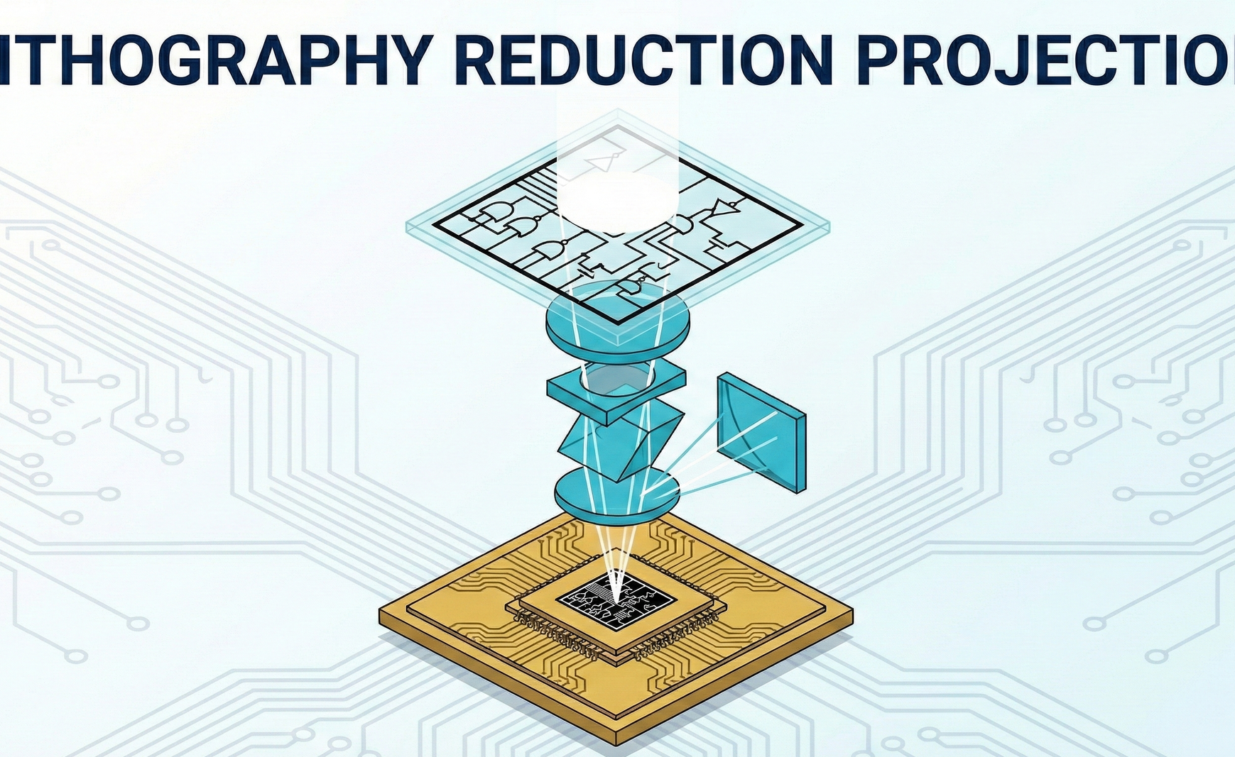
We've all been to the cinema. A projector magnifies a small film strip, projecting it onto a giant screen using light.
The operating logic of a photolithography machine (scanner) is precisely that of an "inverted film projector."
1. Why is "Reduction" Necessary?
In semiconductor manufacturing, there is a golden ratio: 4 : 1.
This means that the circuit pattern on the original mold (reticle) we produce is 4 times larger than the actual pattern on the chip.
- Logic: If you need to create a 3-nanometer line on a chip, directly engraving 3 nanometers onto the mold is too difficult, resulting in a very low yield. However, if we engrave 12 nanometers (4 times larger) onto the mold, it becomes much easier.
- Reduction Projection: After light passes through this "larger" mold, it goes through a set of precision lenses that reduce the image by 4 times, finally projecting it precisely onto the wafer.
- Tolerance: This provides a margin of error for reticle manufacturers. Because tiny imperfections on the reticle, when reduced by 4 times, may become small enough to be ignored.
2. The Carrier of Information: From Virtual to Physical
This process involves the transformation of "information" from one form to another:
- GDSII (Digital File): The design drawing created by engineers on a computer (data of 0s and 1s).
- Reticle (Physical Mask): The data is transformed into chromium metal patterns on glass (a physical stencil).
- Aerial Image (Optical Image): Light passes through the reticle, becoming a patterned light beam (distribution of light wave intensity).
- Resist Image (Photoresist Image): The light beam strikes the photoresist on the wafer, becoming a chemical distribution (latent image).
This is what is known as "transferring the blueprint onto the wafer." This is not physical contact printing, but rather an optical transfer.
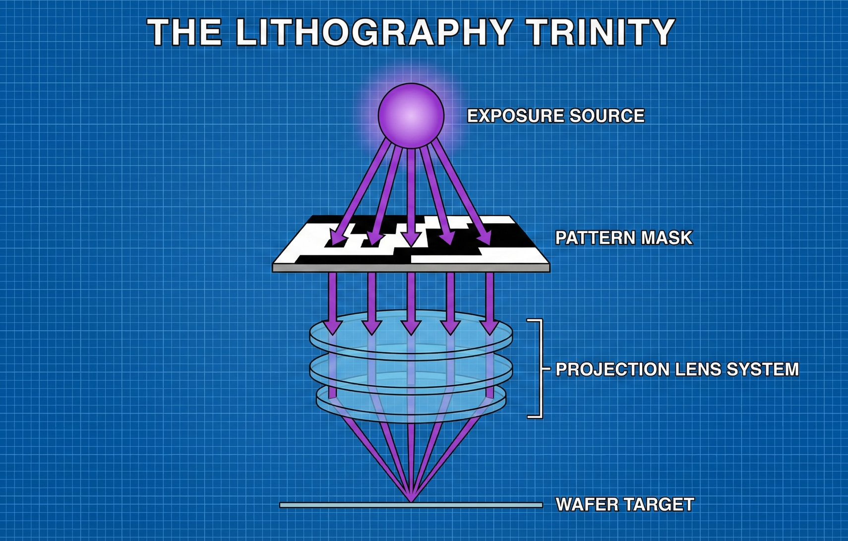
Chapter Two: The Optical Holy Trinity
To accomplish this magic, we need the perfect synergy of three essential components. These three elements define the upper limits of human technology.
1. Light Source — God's Ink
If photolithography is likened to writing, the light source is our ink. The finer the stroke of the ink, the smaller the characters we can write.
In physics, this "stroke thickness" is determined by the wavelength ($\lambda$, Lambda) of light.
- G-line (436nm) / I-line (365nm): Early stages were like drawing with a thick marker.
- DUV (193nm): This was like switching to a ballpoint pen, and it is currently the mainstay for mature processes (7nm - 90nm).
- EUV (13.5nm): This is the ultimate needle tip. The wavelength was instantly shortened by 14 times, allowing us to draw at an atomic scale. This is why ASML's EUV machines are so crucial — they introduced a much finer "ink."
2. Mask / Reticle — The Expensive Slide
The reticle is like a slide in a projector, or a stencil used for spray painting graffiti.
It is typically a 6-inch square quartz glass substrate coated with an opaque layer of chromium metal. Engineers "engrave" the circuit pattern onto the chromium layer; areas where material is removed allow light to pass through, while remaining areas block light.
- Binary Mask: The simplest logic — light (1) or no light (0).
- Phase-Shift Mask (PSM): Advanced magic. By utilizing tiny differences in glass thickness, the "phase" of light is altered, causing light waves to interfere with each other, resulting in sharper edges.
3. Lens System — The Epitome of Focusing
This is the heart of the photolithography machine. After light passes through the reticle, it must go through a lens system to reduce and focus the image.
This is not the kind of lens found in your camera. The lens system built by Zeiss for ASML weighs several tons and consists of dozens of individual lenses, each of which must be polished to near-perfect smoothness.
- Precision Analogy: If this lens system were magnified to the size of Earth, the bumps on its surface could not exceed the thickness of a single strand of hair.
- Mission: It must eliminate all optical aberrations, ensuring that the 4x reduced image remains undistorted in every corner of the wafer.
Chapter Three: The Iron Wall of Physics — Diffraction
Up to this point, it sounds simple: take a light, shine it through a plate, shrink and focus, done.
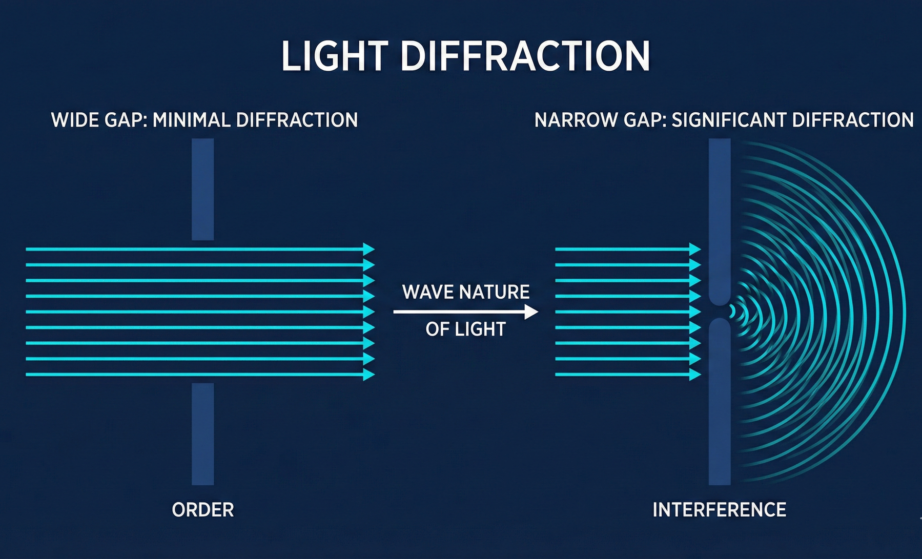
But in the nanometer world, things aren't that simple. Because light is not just a particle moving in a straight line; it is also a wave.
1. When the Door Becomes Narrower Than a Person
Imagine a group of people (light rays) trying to pass through a door (an opening on the reticle).
- Wide Door: If the door is very wide (early micron processes), people can walk straight through, and the shadow outline is very clear.
- Narrow Door: If the door shrinks to allow only one person to pass sideways (advanced processes), people will jostle and spread out in all directions.
This is the phenomenon of diffraction.
When the circuit gap on the reticle (e.g., 10 nanometers) is smaller than the wavelength of light (e.g., 193 nanometers), the light will not shine straight onto the wafer after passing through; instead, it will spread out like ripples.
Result: What should be distinct black and white lines become a blurred gray shadow projected onto the wafer. Two circuits will merge, leading to a short circuit.
2. Rayleigh Criterion — The $E=mc^2$ of the Semiconductor World
To solve this problem, the semiconductor industry adheres to a supreme formula: the Rayleigh Criterion.
$$CD = k_1 \frac{\lambda}{NA}$$
This formula determines the minimum feature size ($CD$, Critical Dimension) we can fabricate on a chip.
To draw finer lines (to make $CD$ smaller), we have only three paths:
- Decrease the numerator ($\lambda \downarrow$): Use light with a shorter wavelength. This is why we need to switch from DUV (193nm) to EUV (13.5nm).
- Increase the denominator ($NA \uparrow$): $NA$ is the numerical aperture, representing the lens's ability to collect light. The larger the lens, the more diffracted light it collects, and the clearer the image. This is why Intel is acquiring High-NA EUV.
- Decrease $k_1$ ($k_1 \downarrow$): This is the magic of process engineers. Through techniques such as Optical Proximity Correction (OPC) and phase-shift masks, they push the boundaries of physical limits.
The entire 60-year history of semiconductors, in essence, is the arduous struggle of hundreds of thousands of engineers dedicating their lives to trying to decrease $\lambda$ and increase $NA$.
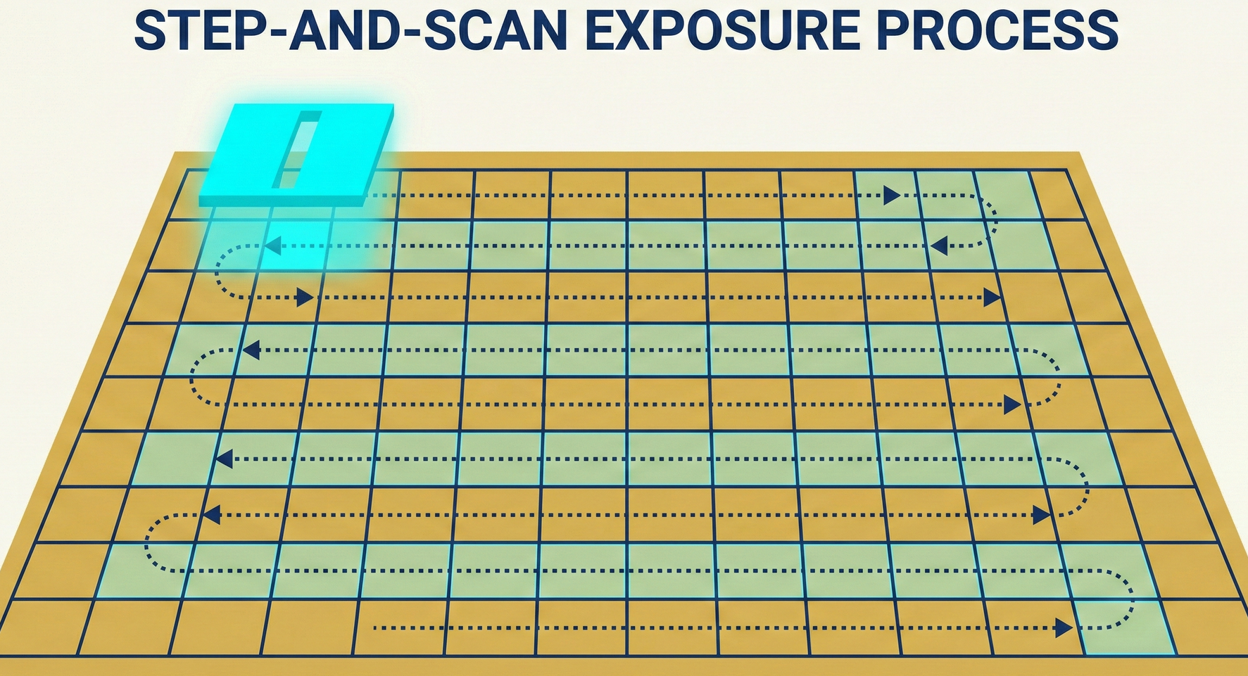
Chapter Four: Step and Scan — The Art of Stamping
Finally, let's discuss how this projection action takes place.
Early photolithography machines were like cameras, capturing the entire wafer in one "click." However, under Moore's Law, wafers grew larger (12 inches) and chips became denser, making it impossible for lenses to simultaneously focus across the entire wafer with nanometer precision.
Thus, we invented the "Step-and-Scan" machine.
1. The Rectangular Exposure Field
The photolithography machine does not expose the entire wafer at once; instead, it divides the wafer into approximately 100 rectangular areas (Shot/Field), each roughly 26mm x 33mm (about the size of a postage stamp).
The lens focuses on processing only this small area at a time.
2. Scanning and Moving
- Scan: When exposing this small area, the reticle stage and wafer stage move synchronously in opposite directions, allowing the light slit to "scan" across the area. This is similar to how a photocopy machine scans a document.
- Step: After scanning one area, the wafer stage quickly moves (Steps) to the next area, where scanning is performed again.
This operation is extremely fast; the wafer stage moves at very high speeds (acceleration can reach G-force levels), yet the positioning error must be controlled within a few nanometers. This is equivalent to a Ferrari braking abruptly from 300 km/h and stopping within 1 millimeter of a cliff edge.
Conclusion: The Magician of Light and Shadow
Photolithography technology is, in essence, a struggle against physics.
We strive to compress grand design blueprints into the microscopic world of silicon atoms.
- The reticle is our film negative.
- The light source is our brush.
- The lens is our magnifying glass (in reverse).
This "100-million-fold reduction" darkroom magic is the cornerstone of modern electronic civilization. Without this 4:1 optical projection logic, there would be no processor in your phone, and no current AI wave.
But optical projection alone is not enough. After light is projected onto the wafer, if it is not "fixed," the image disappears once the light is turned off.
We need a chemical substance that can capture this fleeting light and shadow, transforming it into physical trenches.
This brings us to the most mysterious area in the Fab — the yellow room, illuminated by yellow lights. Please see the next chapter: 2-2-2 The Yellow Room Trilogy: The Chemical Dance of Coating, Exposure, and Development.
In-depth Research · Quantitative Perspective
Want more quantitative research insights on semiconductors?
【Insight Subscription Plan】Break Free from Retail Investor Mentality: Build Your Alpha Trading System with "Quantitative Chips" and "Consensus Data"EDGE Semiconductor Research
📍 Series Map — Navigate the Complete EDGE Semiconductor Research →


