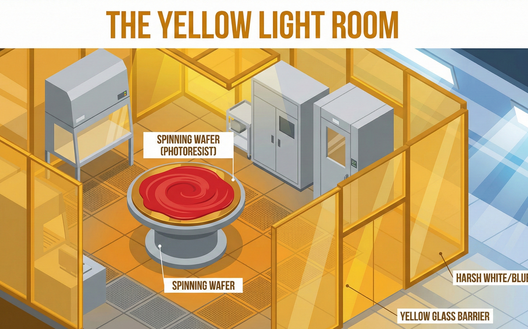
Foreword: Why is it yellow here?
If you have the opportunity to visit a TSMC or Intel fabrication plant (fab), you'll notice that most of the facility's interior consists of vast, pristine cleanrooms. However, in one specific area, the lighting suddenly changes to a dim amber (yellow light).
This isn't for ambiance; it's for survival.
The photoresist we use is a chemical material highly sensitive to light. It acts like traditional camera film, reacting primarily to ultraviolet (UV) light and blue light.
- White light contains blue and violet light. If a photoresist bottle is opened under white light, the entire bottle of chemical will "expose" and be rendered useless within seconds.
- Yellow light (wavelength > 500nm) has lower energy, and photoresist is "blind" to it. Therefore, this is the only safe zone in the fab, and all photolithography-related operations must be completed here.
In this yellow world, wafers undergo a chemical dance composed of three steps. This dance determines the yield of the chips.
Part One: Coating — Nanometer-Scale Spread on Toast
In the first step, we dress the wafer in a photosensitive coat. This might sound like spreading jam on toast, but at the nanometer scale, it's an art that challenges fluid dynamics.
1. Adhesion Promoter (HMDS) — The Perfect Primer
Before applying photoresist, there's a little-known but crucial step: priming.
- Physical Conflict: Silicon wafer surfaces are hydrophilic (water-loving), but photoresists are typically hydrophobic (oil-loving). If you drop photoresist directly onto a wafer, it will bead up like water on a lotus leaf and won't spread evenly.
- Solution: We spray on a layer of gaseous HMDS (Hexamethyldisilazane).
- It acts like a "primer" before applying makeup. It changes the chemical properties of the wafer surface, transforming the wafer, which originally repelled photoresist, into one that can bond tightly with it. Without this step, subsequent patterns would peel off completely during development.
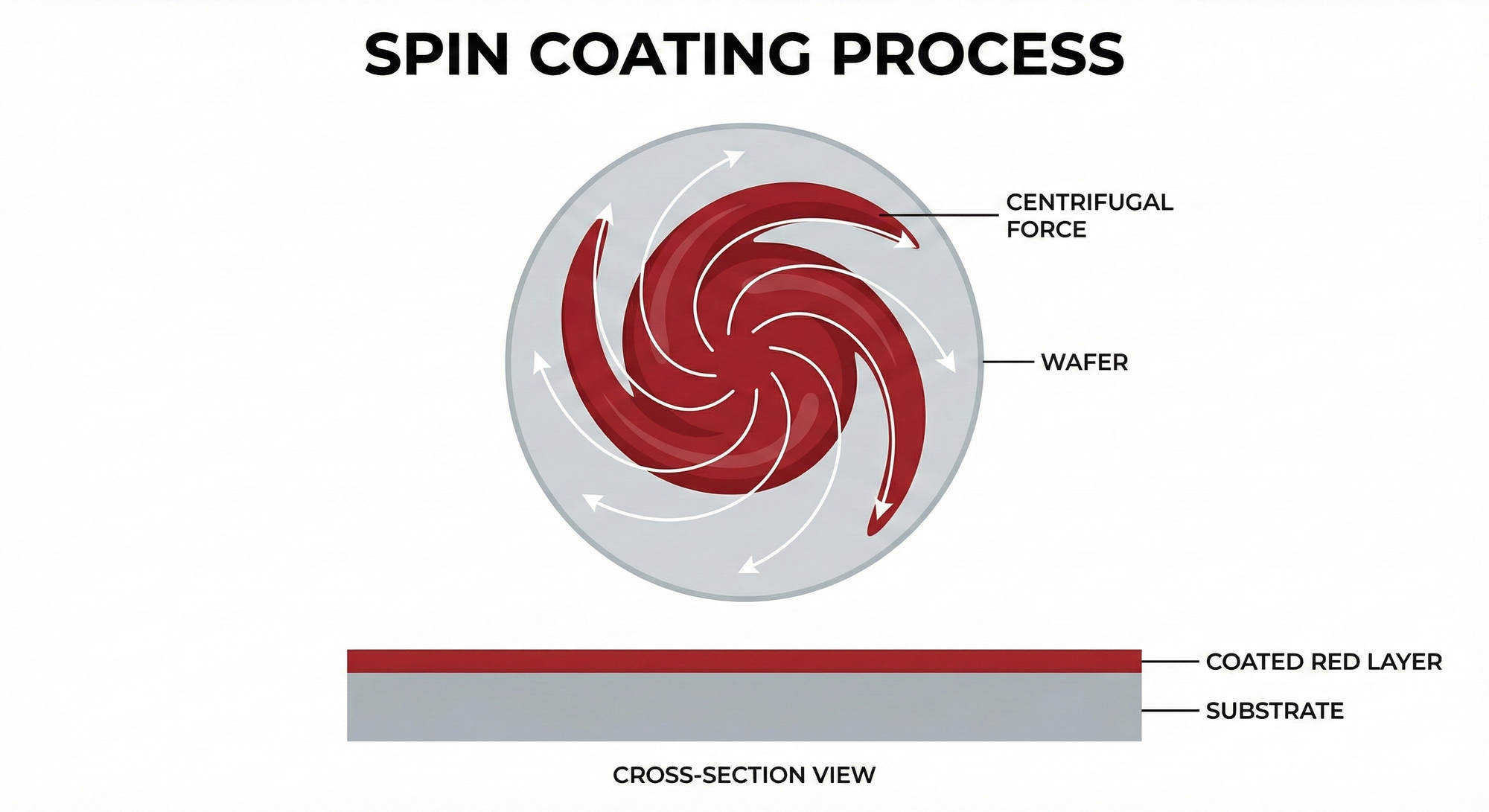
2. Spin Coating
Next is the main event. The wafer is secured by a chuck onto a high-speed rotating spinner.
- Dispensing: A robotic arm dispenses a drop of viscous photoresist liquid, similar to honey, right at the center of the wafer.
- Spinning: The spinner instantly accelerates to 3,000 to 5,000 revolutions per minute (RPM).
- Centrifugal Force: Powerful centrifugal force flings the photoresist liquid outwards, covering the entire wafer.
The Ultimate Challenge: Uniformity
This film's thickness is typically only a few hundred nanometers. The critical point is that the thickness variation between the center and the edge must not exceed 1-2 nanometers (roughly the thickness of a few atomic layers).
Why? Because if the thickness is uneven, the light penetration depth will vary, leading to circuits that are inconsistently deep or shallow, ultimately rendering the chip unusable.
3. Soft Bake
Newly coated photoresist is still in liquid form and contains a large amount of solvent. We must transfer it to a hot plate for baking (approximately 90-100°C).
- Purpose: To evaporate the solvent, transforming the photoresist from a liquid into a solid film.
- Edge Bead Removal (EBR): During the spinning process, a thicker ring of photoresist accumulates at the wafer edge due to surface tension (like a pizza crust). This must be removed using chemical solvents, otherwise, it will affect subsequent focusing.
Part Two: Exposure — The Invisible Chemical Lock
The wafer exits the coater (track) and travels via automated tracks into the belly of the lithography machine (scanner). This is the moment when the optical projection mentioned in 2-2-1 occurs, but here, our focus is on what happens chemically.
1. Alignment — Fastening the First Button
The most difficult part before exposure isn't illuminating, but alignment.
Modern chips have 60 to 80 layers of circuitry. Like constructing a building, the circuitry on the 50th layer must be perfectly stacked on top of the 49th, and the interconnecting holes (Vias) must precisely align.
- Overlay Error: This is a yield killer. If one layer is shifted to the left and the next to the right, the circuit will be broken.
- Precision: In a 3-nanometer process, the allowable error range is only 1-2 nanometers. ASML's machines must locate tiny "alignment marks" on the wafer and adjust the wafer stage position within milliseconds.
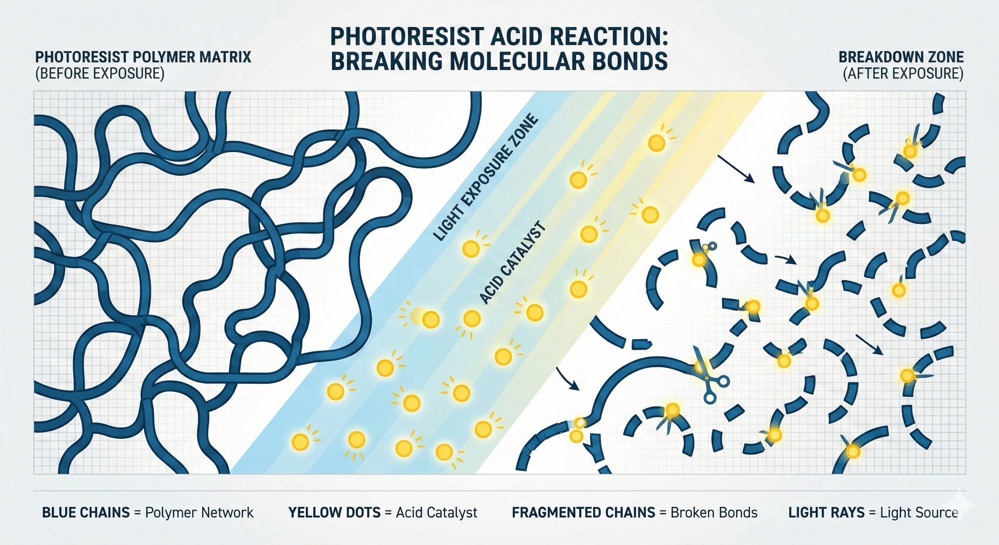
2. Latent Image — Schrödinger's Cat
Once alignment is complete, intense light (DUV or EUV) passes through the photomask and strikes the wafer.
At this point, something magical happens: you see no visible changes.
The wafer surface still appears the same color. However, in the microscopic world, the PAG (Photoacid Generator) inside the photoresist has already been activated.
- Acid Release: In the areas exposed to light, PAG decomposes and releases trace amounts of "acid".
- Precursor to a Chain Reaction: These acids are currently dormant; they are the catalysts for the next stage of chemical reaction. This is known as a "latent image"—the image exists, but it has not yet become visible.
3. Post Exposure Bake (PEB)
This is the most critical chemical moment. The wafer is once again transferred to a hot plate (approximately 110-120°C).
- Acid Diffusion: Driven by thermal energy, the newly generated acids begin to move around like little sprites.
- Scissors: These acids cleave the polymer chains of the photoresist, transforming originally long, water-insoluble molecules into short, water-soluble ones.
- Standing Wave Effect: Light reflects within the photoresist, causing uneven exposure due to peaks and troughs. The thermal energy from PEB also helps to smooth out this physical imperfection.
Part Three: Development — The Truth Revealed
After coating and exposure, the circuit pattern on the wafer is still invisible. Now, we need to "develop" it.
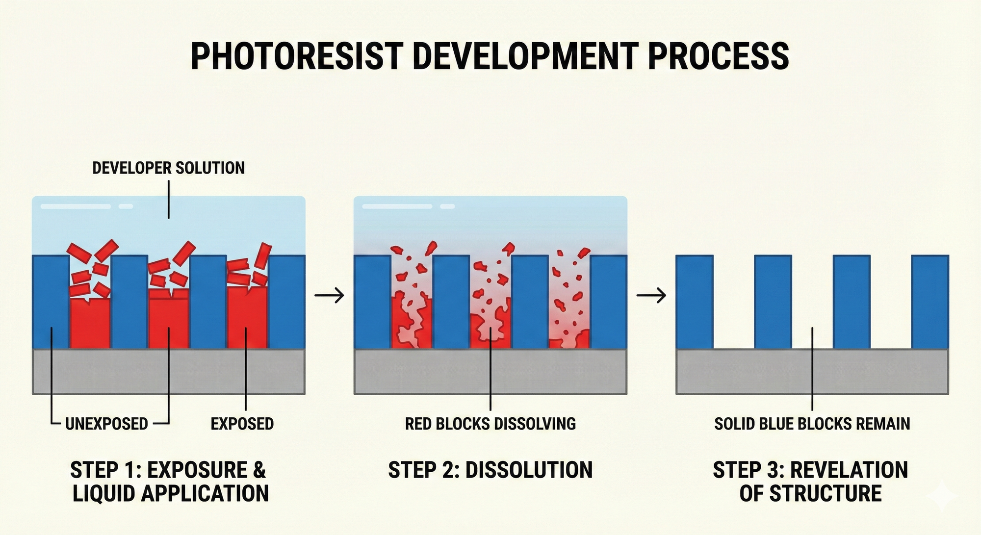
1. Developer — The Alkaline Baptism
The wafer returns to the coater-developer track. Nozzles spray developer onto the wafer surface (typically TMAH, Tetramethylammonium Hydroxide, a strong base).
- Fate of Positive Resist:
- Do you recall the molecules cleaved by acid during the PEB stage? Those were the areas exposed to light.
- These shortened molecules are highly soluble in the alkaline developer.
- Result: The areas exposed to light disappear, forming trenches. The unexposed areas remain, forming walls.
- This is the dominant logic in current advanced processes.
- Reversal in Negative Resist:
- Used in earlier or specialized processes.
- The logic is opposite: areas exposed to light harden (cross-linking reaction), while unexposed areas are washed away.
2. Puddle Development
To conserve expensive developer and ensure uniformity, modern processes employ "puddle development."
- After the nozzle dispenses the liquid, surface tension allows the developer to form a puddle covering the wafer surface, where it sits for several tens of seconds.
- This allows the chemical reaction to proceed fully and dissolves waste material.
- Finally, deionized water (DI Water) is sprayed to rinse it clean, followed by high-speed spinning to dry.
3. Hard Bake and Inspection
Finally, the wafer is baked again to thoroughly harden the remaining photoresist patterns. Because next, they will face the most brutal test—etching. The photoresist must act like bulletproof armor, protecting the underlying silicon wafer from strong acids or plasma corrosion.
ADI (After Develop Inspection): The Last Chance to Rework
- Why is it important? This is the only step in the semiconductor manufacturing process where "rework" is possible.
- If issues are detected, such as improperly coated photoresist, incomplete development, or misaligned patterns, engineers can strip off the entire photoresist layer, then recoat and re-expose.
- Once this stage is passed and etching begins, the silicon wafer is physically altered, and the process becomes irreversible.
Conclusion: The Gatekeeper of Yield
This "coating → exposure → development" process flow must be repeated 60 to 80 times during the manufacturing of a single chip (because chips have dozens of layers).
Each cycle must be flawless.
- A single speck of dust falling into the coater can cause an open circuit.
- A 0.5-degree difference in hot plate temperature can alter the photoresist reaction rate, causing line width deviations.
- A clogged developer nozzle can result in residual photoresist.
This is the essence of the yellow light area: it's not just about operating machines; it's about the ultimate control of chemistry, fluid dynamics, and thermodynamics. If ASML's lithography machines are God's paintbrush, then the engineers in the yellow light area are the master artists responsible for mixing the colors, preparing the canvas, and ensuring every stroke is precisely placed.
Now, the canvas is ready, and the patterns have emerged. But these are only soft photoresist patterns.
Next, we need more powerful forces to truly "etch" these patterns into the very core of the silicon wafer. But before that, we must first learn about the "arms dealer" who provides "God's paintbrush"—2-3 God's Paintbrush: Lithography Machines and Pattern Definition.
In-depth Research · Quantitative Perspective
Want to gain more insights into semiconductor quantitative research?
[Insight Subscription Plan] Bid Farewell to Retail Investor Mindset: Build Your Alpha Trading System with "Quantitative Chips" and "Consensus Data"EDGE Semiconductor Research
📍 Series Map — Navigate the Complete EDGE Semiconductor Research →


