2-3-2 The Final Gamble — Intel 14A vs. TSMC A16: The Roadmap Battle
ASML's High-NA EUV boosts resolution via anamorphic lenses, halving exposure fields and causing chip stitching. This sparks a battle: Intel bets on new machines for tech lead; TSMC uses older machines, multi-patterning for cost/yield. Photoresists need metallic scaffolds. Short-term, TSMC wins av...
We want $CD$ (linewidth) to be as small as possible, yet the variables we can manipulate are surprisingly few:
$\lambda$ (Wavelength) — Dead End: We barely managed to shrink it from 193nm (DUV) to 13.5nm (EUV). Want to shorten it further? That would require entering the X-ray domain, which current materials physics cannot possibly handle. This path is blocked.
$k_1$ (Process Factor) — Squeezed Dry: This is TSMC's strength. Through various optical proximity correction (OPC) techniques, $k_1$ has been pushed close to the physical limit of 0.25. This is like wringing a wet towel until not a single drop of water remains. This path is also nearly exhausted.
$NA$ (Numerical Aperture) — The Only Salvation: In the formula, only the denominator $NA$ can be manipulated. By increasing the denominator, $CD$ will decrease.
What is NA (Numerical Aperture)?
Simply put, it is the 'opening angle' of the lens, and also represents the lens's 'ability to capture detail'.
Imagine you are using a fishing net to catch fish (capturing information from light diffraction).
Low-NA (0.33): The net's opening is medium-sized, only catching the main fish, while small fish (minute circuit information) will slip through.
High-NA (0.55): We stretch the net super wide, capturing all the detailed light that would otherwise escape.
This is why Intel is willing to spend $380 million to purchase this machine. Because beyond this, Moore's Law has no path forward.
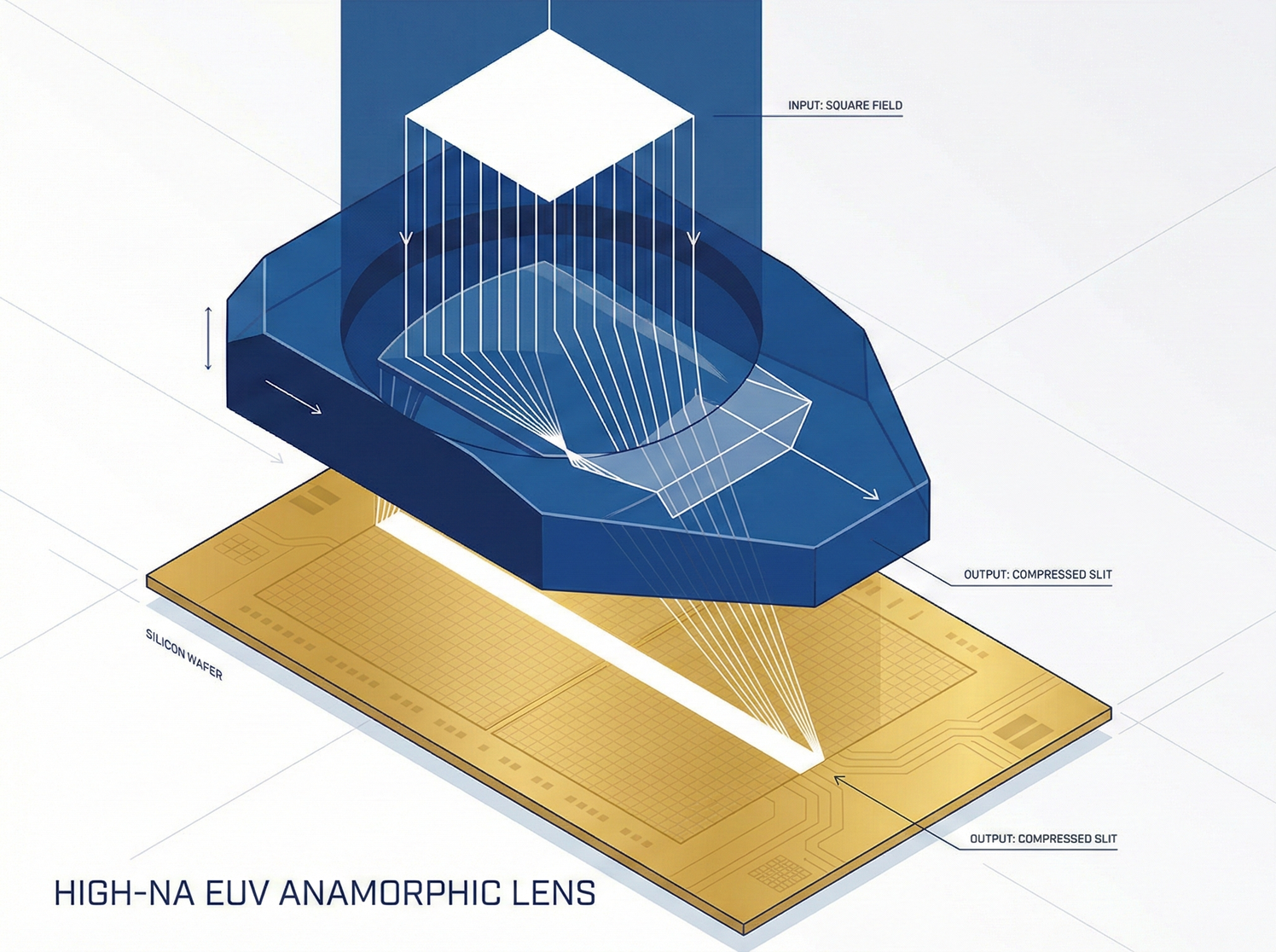
🔭 Chapter One: The Price of a Giant Lens — Anamorphic Optics
Increasing NA from 0.33 to 0.55, does it just sound like swapping for a larger lens?
Wrong. This is an optical design catastrophe.
To capture a wider angle, the mirrors must become **super huge**. This leads to a severe geometric problem: **the incident angle of light is too large, causing the reflected light paths to interfere with each other (Obscuration).** If we maintain the original design, the mirrors would block their own light.
1. Zeiss's Solution: Anamorphic Lens
To resolve this physical conflict, ASML and Germany's Zeiss collaborated to create an astonishing design: the **"anamorphic lens"**.
They no longer pursued perfect symmetrical reduction; instead, they created an "aspherical funhouse mirror":
X-axis: Maintains 4x reduction (same as before).
Y-axis: Becomes 8x reduction.
Analogy for Beginners: "Cinemascope"
This is similar to the technique previously used in movie theaters to fit a wide image into a narrow film strip.
The patterns on the photomask, originally square, are "unidirectionally flattened" when projected onto the wafer after passing through this "funhouse mirror." If uncorrected, an originally circular hole would be printed as an oval. Engineers must first stretch the pattern in the software to counteract this distortion.
2. Fatal Flaw: Half-Field Exposure
While the anamorphic lens solved the problem of light path interference, it introduced a side effect that causes TSMC to frown: Half-Field Exposure (High-NA Half-Field).
This is High-NA's most fatal drawback.
Because the Y-axis is compressed by 8 times (originally 4 times), the effective area projected onto the wafer is directly **halved**.
Standard EUV (Low-NA): The area exposed in one "snap" is 26mm x 33mm (full-field).
High-NA EUV: The area exposed in one "snap" is reduced to just 26mm x 16.5mm (half-field).
How severe are the consequences?
Consequence One: Halved Capacity, Soaring Costs
An area that could originally be covered in one exposure now requires two. The wafer stage's movement count doubles, directly halving capacity. For fabs where every second counts, this is simply burning money.
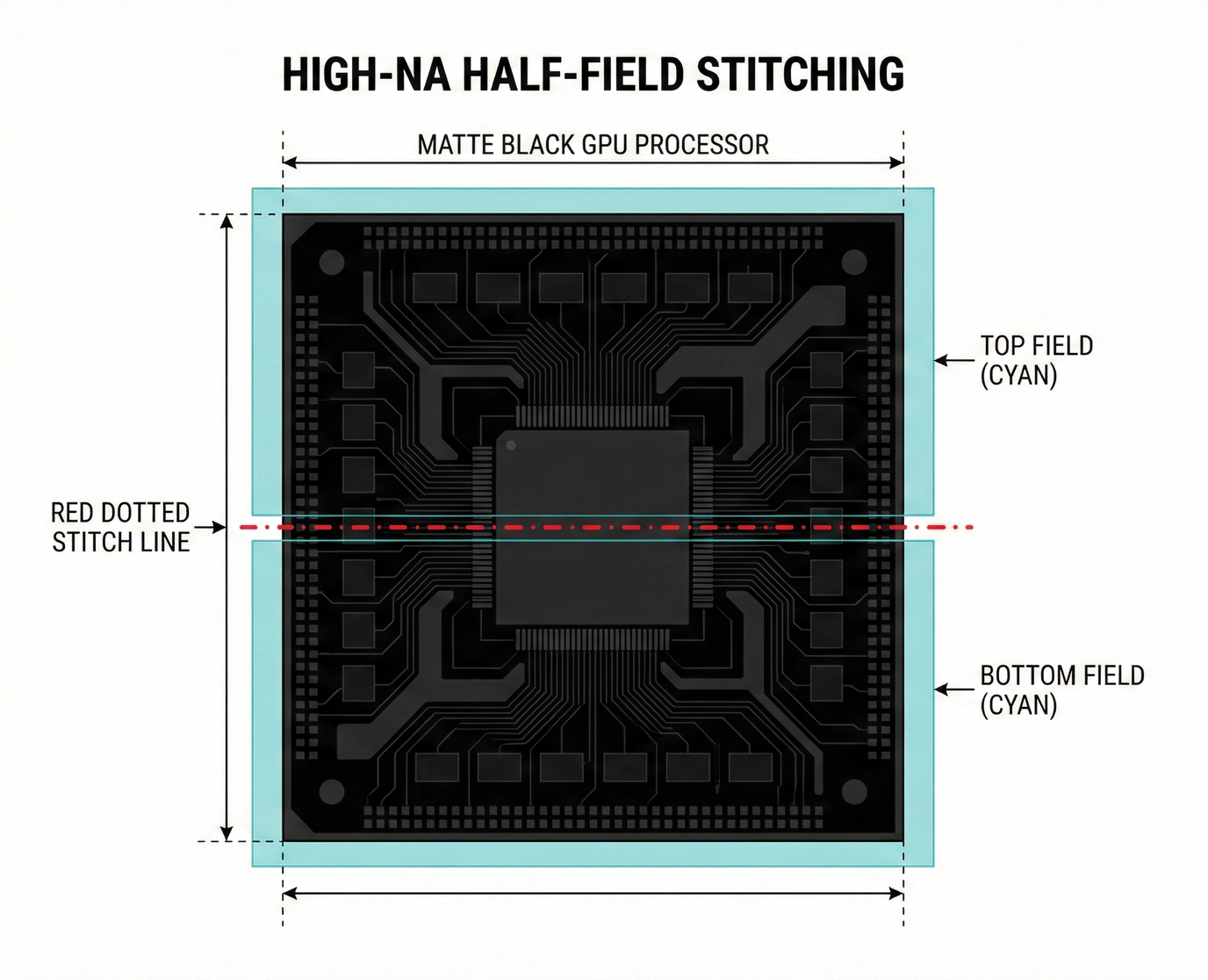
Consequence Two: Designers' Nightmare — Stitching
This is what truly frustrates customers like NVIDIA.
Consider the popular NVIDIA B200 (Blackwell) chip; its size is enormous, with an area approaching the 26mm x 33mm limit.
Printed with older machines: Fits perfectly within one exposure field, ideal.
Printed with High-NA:Doesn't fit! The chip is larger than the exposure frame.
What to do?
The only solution is to **cut the B200 design in half**.
First, print the top half, then move the wafer, print the bottom half, and then "stitch" them together during the packaging stage.
This sounds simple, but in the nanoscale world, it's like dancing on a razor's edge.
This "stitch line" must be accurate down to the atomic level. Even a slight misalignment would render the entire $40,000 GPU worthless.
This is why TSMC has been reluctant to adopt High-NA — who wants to buy a chip that's been cut in half and then glued back together?
⚔️ Chapter Two: Intel 14A vs. TSMC A16 — The Battle of Roadmaps
This is the generational gambit between Pat Gelsinger and C.C. Wei. It's not just a technological showdown, but a clash of two management philosophies: "buying time with money" vs. "leveraging technology for cost efficiency".
This post is for subscribers only
Sign up now to read the post and get access to the full library of posts for subscribers only.