💡 Core Question: The Cliff Between Virtual and Reality
In the long journey of chip design, the moment engineers press the "Sign-off" button on EDA software, we stand at the edge of a dangerous cliff.
On this side of the cliff is the perfect digital world. The chip exists merely as vast amounts of 0s and 1s (GDSII files) in a computer, with perfectly straight lines and flawless logic. But on the other side of the cliff is the cruel physical world. There, we encounter light diffraction, chemical diffusion, and interference from dust.
To bridge this chasm, we must transform these virtual digital signals into physical "atomic molds." This converter is an extremely expensive, yet little-known, critical consumable in semiconductor manufacturing—the photomask.
🔦 Part One: The Birth of the Photomask — The Slow Dance of the Electron Beam
The Master Stencil — The "Negative" of the Chip
Many industry observers have heard of photomasks but find it hard to imagine exactly how they work. A physical photomask is a quartz glass plate, approximately 6 inches square (15 cm) and 0.6 cm thick. Its surface is covered with black circuit patterns drawn using "chrome."
In a lithography machine, it acts like a slide; but before it enters the lithography machine, it must first be "manufactured." And this is the most arduous step.
1. The Chicken-and-Egg Problem: Who Makes the Photomask?
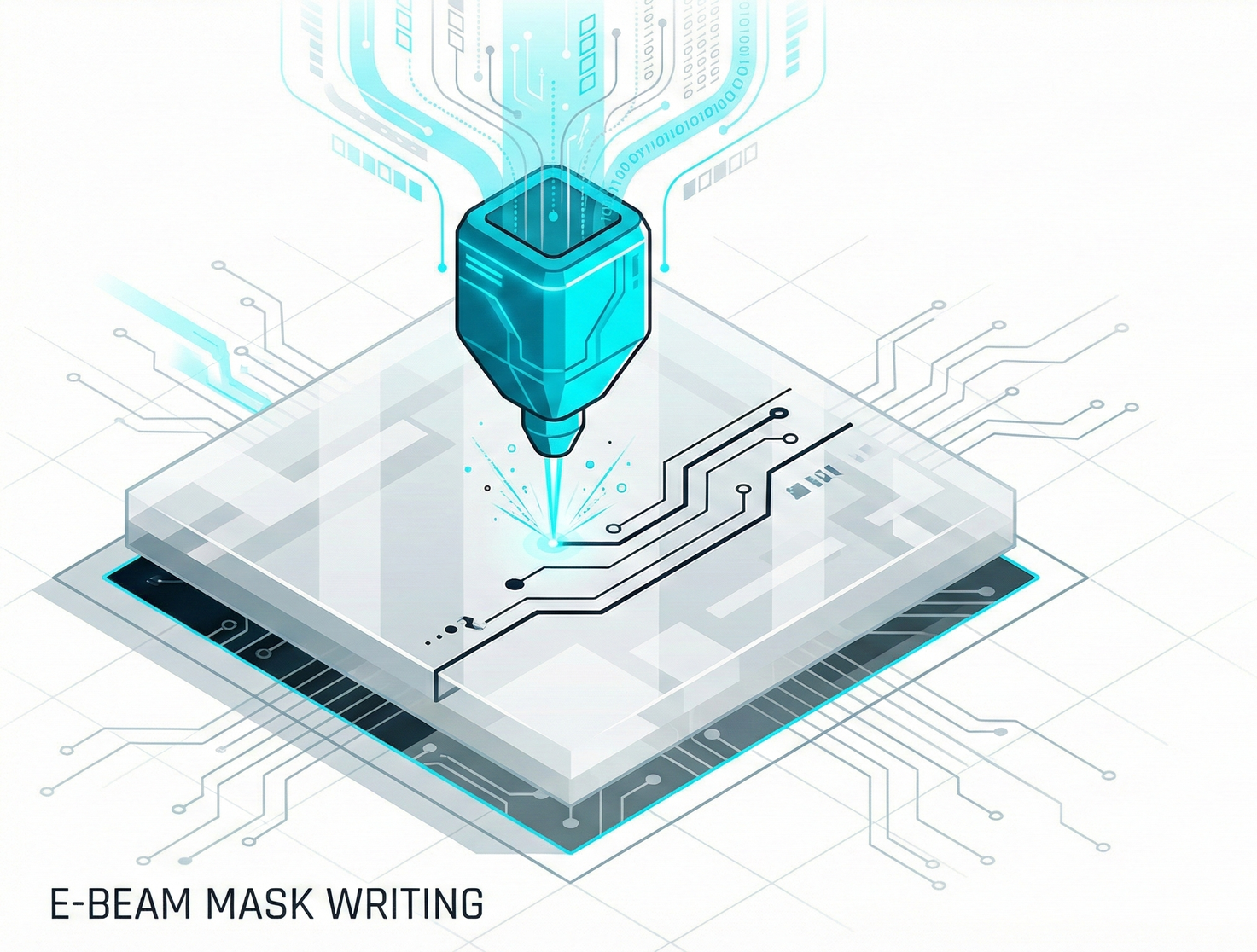
We use lithography machines to print chips, so who prints the photomasks? The answer is: we can't "print" them; we must "write" them.
This is the job of the Electron-Beam Writer (E-Beam Writer).
- Wafer Lithography (Scanner): Like stamping. A flash of light, a "click," and billions of circuit patterns are simultaneously printed on the wafer. Extremely fast.
- Mask Writing (Mask Writer): Like transcribing the Bible with a ballpoint pen. The electron beam must act like a nano-scale pen, meticulously drawing the patterns pixel by pixel, line by line, on a blank quartz glass substrate.
2. The Weight of Data: Hundreds of TB of Handwritten Manuscripts
At the 3nm process, the complexity of patterns on a single photomask already surpasses human imagination.
- Data Volume: The data volume for a single critical photomask layer can be as high as hundreds of TB.
- Time Cost: To ensure every nanometer pixel is perfectly precise, the electron-beam writer must work slowly and meticulously. Writing a single perfect photomask often requires days and nights of uninterrupted scanning.
This is why photomasks are so expensive (a set costs hundreds of millions of New Taiwan Dollars). It's because virtual-world data is etched into real-world glass, stroke by stroke, in the slowest and most precise manner possible.
🔮 Part Two: Computational Lithography — The Art of Deceiving Physics
If the electron beam simply drew the design on the photomask as is, this game would be easy. But physics likes to play tricks.
The "Fat Finger" Effect of Light Imagine trying to draw a "hair" (a 3nm circuit) on paper with a "thick-tipped marker" (a 193nm light source). When light passes through extremely narrow slits on the photomask, it doesn't travel in a straight line but "diffracts" and spreads out like water waves.
- Result: You draw a perfect "square" on the photomask, but when projected onto the wafer, it becomes a blurry "circle," or even smears together, making it non-conductive. This is known as Optical Proximity Effect (OPE).
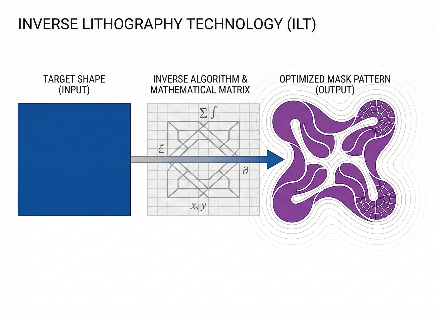
1. From OPC to ILT: The Birth of Alien Symbols
Since we cannot change the laws of physics (the wavelength of light), engineers decided to "trick" it. This is the battlefield of Computational Lithography.
- Basic Magic: OPC (Optical Proximity Correction) Engineers intentionally draw an extra protruding shape at the corners of right angles (known in the industry as Hammerhead or Dog-bone).
- Principle: Since light rounds off corners, I'll draw the corners extra sharp. After erosion, they'll become perfect right angles.
- Advanced Magic: ILT (Inverse Lithography Technology) In advanced processes, simple corrections are no longer effective. We must use ILT (Inverse Lithography Technology). This is reverse thinking: we no longer ask, "What will this drawing turn out to be?" Instead, we ask the computer: "I want a perfect square on the wafer; what should the photomask look like?" After billions of simulation calculations, the computer's answer will astound you: The patterns on the photomask are no longer straight lines and squares but a collection of random, curvilinear, mosaic-like "alien symbols."
- Visual Impact: These patterns don't resemble circuits at all; they look like "mathematical totems" born to accommodate the physical properties of light. Only when light passes through these strange symbols does it reconstruct the desired circuits on the wafer.
2. The Computational Black Hole and NVIDIA's Entry
The price of this "deceiving physics" is an immense amount of computing power. Calculating the ILT patterns for an entire chip requires tens of thousands of CPU servers to run continuously for several weeks. This has become one of the longest bottlenecks in the chip design cycle.
This is why NVIDIA made a big move in 2023, launching its cuLitho library.
- Jensen Huang's Logic: Since these are all matrix computations, why use CPUs?
- Transformation: By leveraging the parallel computing power of GPUs, NVIDIA accelerated this computation process by 40 times. What used to take two weeks to calculate for photomask patterns now only takes one night.
This is a perfectly ironic closed loop: we need the most powerful AI chips (like H100) to provide the computing power to calculate the photomask patterns required for the next generation of AI chips. Chips are making themselves.
⚔️ Part Three: The Deep End — From Window to Magic Mirror (The Bragg Reflector)
As manufacturing processes cross the 7nm node, the light source wavelength shortens to 13.5nm (EUV). At this moment, the physical logic of optical lithography undergoes a paradigm shift. We are no longer looking through a window; instead, we must create a perfect magic mirror in the dark.
1. Physical Obstacle: The Light of Death
In the 193nm (DUV) era, we used quartz glass because light could pass through it.
However, 13.5nm extreme ultraviolet (EUV) light is the "light of death" in physics. Almost all matter in the universe—air, water, glass, lenses—strongly absorbs light in this wavelength band.
- Conclusion: Transmissive masks are dead.
- Solution: The only way is to make the light "reflect" back.
2. The Bragg Reflector — Deceiving Light Interference
This sounds simple: just put up a mirror, right?
Wrong. Ordinary metal mirrors (like silver or aluminum) are like black paper to EUV, absorbing it just the same.
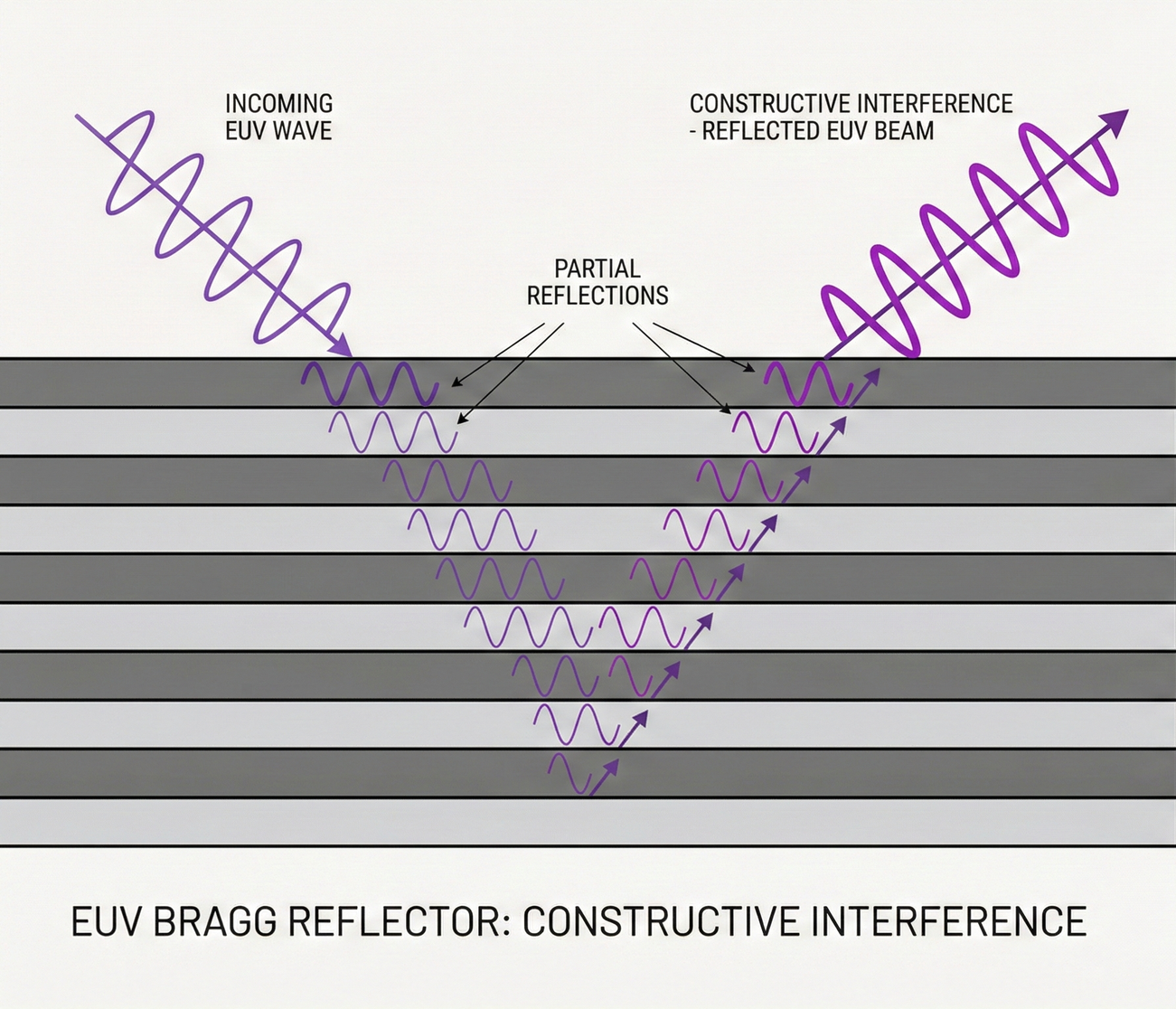
To reflect this tricky light, humanity was forced to construct an "artificial crystal" at the atomic scale: the Bragg Reflector (Distributed Bragg Reflector, DBR).
- Structure: On the EUV photomask substrate, Molybdenum and Silicon are alternately stacked. Typically, 40 to 50 pairs are needed, which means 80 to 100 layers.
- Principle (Constructive Interference): The thickness of each layer must be extremely precisely controlled to a $\lambda / 2$ period (approximately 6.9nm, single layer about 3.4nm).
- A single Molybdenum-Silicon interface can only reflect a tiny amount of light.
- But when 80 layers of reflected light waves have their "crests" perfectly aligned, they undergo resonance.
- This is like 80 faint voices singing in unison, converging into a loud, strong beam of light (reflectivity reaching ~70%).
3. Nightmare: Phase Defect and the Princess and the Pea
This structure brings about one of the most terrifying nightmares in semiconductor manufacturing—phase defects.
Imagine the fairy tale "The Princess and the Pea": a single pea hidden under 20 mattresses can make the princess sleeping on top feel a bump.
On an EUV photomask, if there is an atomic-sized bump on the substrate (even smaller than a virus), the 80 layers of Molybdenum-Silicon thin film deposited above it will also bulge.
- Consequence: When light hits this bulge, even though it reflects, its "phase" is disrupted (the optical path difference changes).
- Ghost Image: This phase-incorrect light will undergo "destructive interference" with the surrounding normal light. The result: even though there is no pattern on the photomask, a mysterious black spot or open circuit is printed on the wafer.
- Zero Tolerance: This type of defect is "unrepairable." Therefore, an EUV photomask substrate must be perfectly Zero Defect. This is why Japan's HOYA dominates the substrate market.
🛡️ Part Four: The Pellicle War — A Billion-Dollar Decision
Given that photomasks cost hundreds of thousands of US dollars, common sense dictates we would add a transparent protective cover to them—this is the pellicle. Its function is to block dust, causing particles to settle out of focus so they aren't printed on the wafer.
However, in the EUV era, this life-saving film triggered a monumental standoff between TSMC and ASML.
1. A Dilemma: Life or Money?
EUV light is too delicate; even the pellicle absorbs it.
Worse still, light passes "twice" through the reflective photomask (once when entering, once when reflecting out). This effectively doubles the absorption.
- Assuming the pellicle transmittance is 90%, after two passes, only 81% ($0.9 \times 0.9$) remains.
- Cost: Light intensity is reduced by nearly 20%, meaning exposure time must be lengthened, and throughput directly drops by 20%. For wafer fabs where every second counts, this is an unacceptable loss of profit.
2. TSMC's Bold Gamble: Going "Naked"
In the early stages of 7nm and 5nm mass production, TSMC made an industry-shocking, high-stakes decision: We will not use a pellicle.
- ASML's Warning: "You're crazy! If even a single speck of dust falls on the photomask, the entire batch of wafers will be scrapped."
- TSMC's Logic: Rather than losing 20% of throughput, we will make our cleanrooms "obsessively" clean. At the same time, we will develop an ultra-high frequency "E-Beam photomask inspection and cleaning" process.
- Result: TSMC won the gamble. This "naked strategy" allowed TSMC to squeeze out higher throughput and yield than its competitors in the early days when EUV light source power was not yet strong enough (at that time, the light source was 250W or even lower). This was a triumph of operational management.
3. The Salvation of New Materials: Carbon Nanotubes (CNT)
However, as processes advance to 3nm and 2nm, circuits are extremely miniaturized, and any nanometer-scale contamination is intolerable. Coupled with light source power increasing to over 350W, the photomask surface temperature is extremely high, eventually requiring us to put the "clothes" back on.
Currently, ASML, Imec, and microelectronics centers are developing the next generation of pellicles:
- Material Holy Grail: Metal Silicide or Carbon Nanotubes (CNT).
- Demanding Requirements: These pellicles must be as thin as a cicada's wing (transmittance >90%) while being able to withstand instantaneous high temperatures of 1000°C without breaking. This itself is a pinnacle challenge in material science.
💰 Part Five: The Business Moat — NRE and the Capital Filter
Understanding the physical limits allows us to comprehend the commercial realities.
The exponential upgrade of photomask technology has directly led to the "gentrification" of chip design entry barriers. This industry is becoming a club accessible only to the ultra-wealthy.
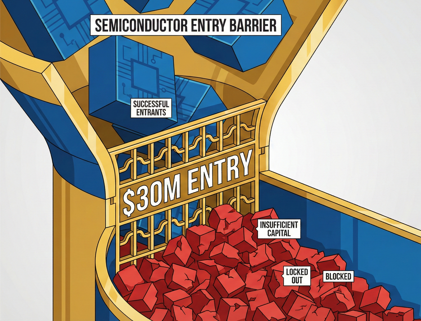
1. Components of NRE (Non-Recurring Engineering)
When making a chip, the most expensive part is often not "production" (variable cost) but the initial "tooling cost" (fixed cost), which is NRE.
And within NRE, the most astonishing expense is the Mask Set.
- 28nm: A mask set costs approximately NT$30 million. Many medium-sized design companies can afford this.
- 3nm: A mask set's cost has soared to NT$1 billion (approximately US$30 million).
- This means you're already in debt by NT$1 billion before selling a single chip.
2. The Capital Filter
This exorbitant threshold creates a strong "filtering effect":
- The Rich Get Richer: Only companies like Apple, NVIDIA, and Qualcomm, whose shipments are in the "hundreds of millions" of units, can amortize this cost.
- If 100 million units are sold, the photomask cost allocated per chip is only NT$10. This is almost negligible.
- Startup Graveyard: If you are an AI startup, estimating chip sales of only 100,000 units.
- Each chip would have to bear NT$10,000 in photomask costs.
- This makes your chip cost several times higher than competitors', making it unsellable.
3. The Only Lifeline: MPW (Multi-Project Wafer)
So, what about academia and startups?
The only way out is called MPW (Multi-Project Wafer), commonly known as "the Uber Pool of the chip industry."
- Logic: Since a single photomask is so expensive, we combine the circuit designs from National Taiwan University, National Tsing Hua University, and several small companies all on the same photomask.
- Advantage: The NT$1 billion cost is shared by 20 companies, with each paying only NT$50 million.
- Disadvantage: You only receive a small number of samples, and the waiting time is long. But this is the only narrow path to advanced processes.
📝 Strategic Summary
- The Pinnacle of Physics: EUV photomasks are no longer mere optical components but "quantum resonance cavities" constructed from 80 atomic layers.
- The Operational Gamble: The Pellicle War proves that semiconductor victories often come from engineering courage to challenge standard procedures (like TSMC's "naked" approach).
- The Capital Barrier: Photomask prices are growing exponentially. This dictates that advanced processes will be a game of oligopoly, with companies lacking economies of scale blocked by high walls.
In-Depth Research · Quantitative Perspective
Want more insights into semiconductor quantitative research?
【Insight Subscription Plan】Break Free from Retail Investor Mindset: Build Your Alpha Trading System with "Quantitative Chips" and "Consensus Data"EDGE Semiconductor Research
📍 Series Map — Navigate the Complete EDGE Semiconductor Research →


