Foreword: Liquid Film, Solid War
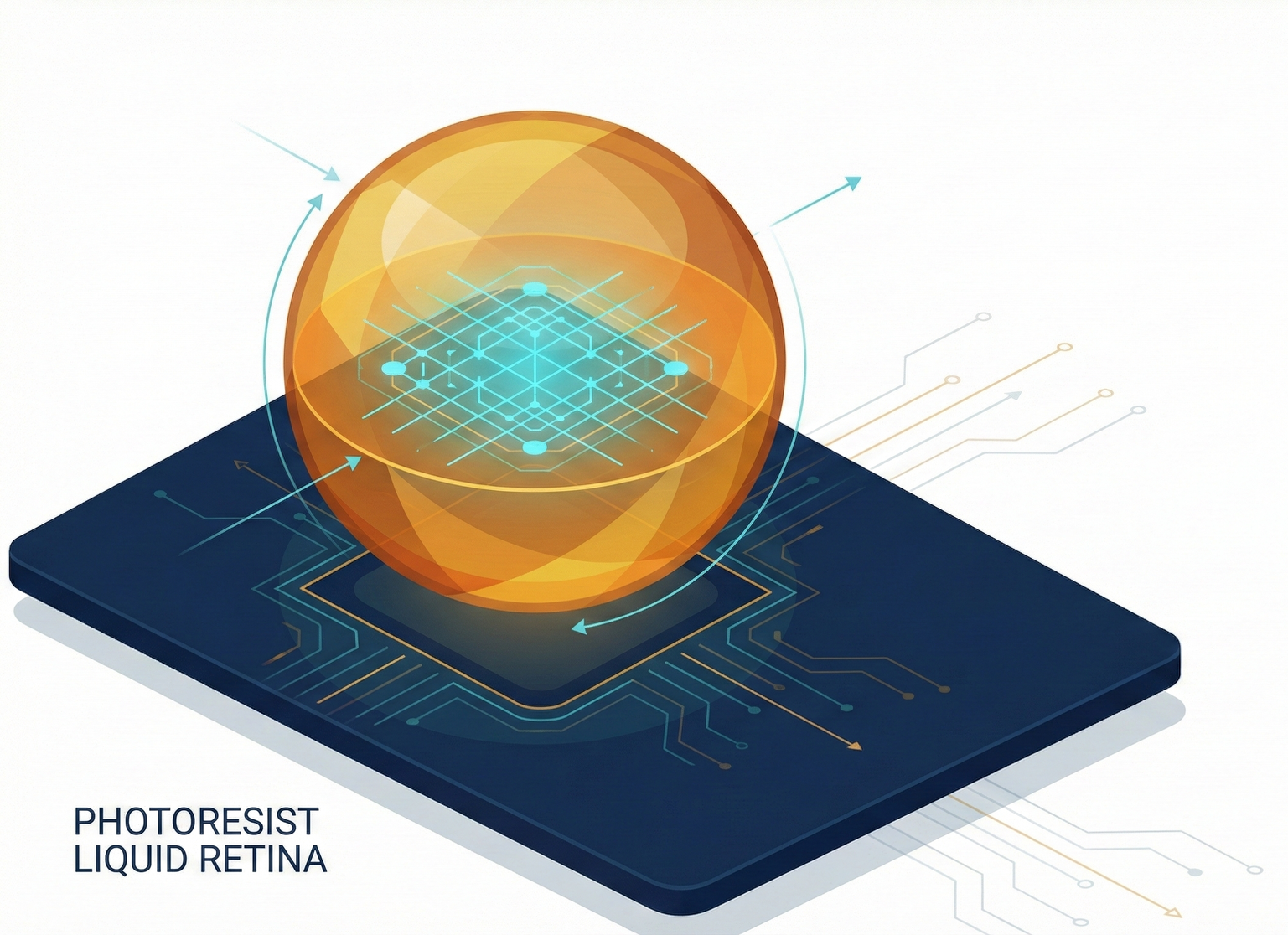
If ASML's EUV lithography machine is God's paintbrush, then photoresist is the most critical "retina" on this canvas.
Imagine this scenario: ASML's machine weighs 180 tons, costs NT$4.8 billion, and after reflecting through dozens of Zeiss lenses internally, finally projects that precious 13.5nm light beam onto the wafer. If the quality of this liquid photosensitive material is not good enough, this machine would instantly turn into "the most expensive toaster in history."
In semiconductor materials science, photoresist is the jewel in the crown. Not only must it be capable of chemical reaction, but it must also be "abnormally pure."
- General industrial standard: 99.9% (3N).
- Semiconductor standard: PPT (Parts Per Trillion) level.
- Concrete analogy: This is equivalent to searching for a specific one-dollar coin across the entire surface of the Earth; or detecting a single drop of ink in 20 Olympic-sized swimming pools.
- Why? Because in a 3nm gate structure, the presence of just one sodium ion (Na+) or iron ion (Fe+) can cause transistor electrical drift, rendering the entire chip unusable.
This is a precise war waged in liquid, and Japan is the sole arms dealer in this conflict.
🖌️ Chapter One: Chemically Amplified Resist (CAR) —— A Microcosmic Chain Nuclear Explosion
Before delving into advanced processes, we must first understand the core mechanism of modern photoresists. Early photoresists (such as those from the G-line/I-line era) adopted a "one-to-one" reaction logic: one photon strikes, changing the structure of one molecule.
However, in the EUV era, this logic no longer works.
- Pain point: EUV light sources are extremely expensive and weak. If relying on traditional photosensitive mechanisms, exposure times would become very long, causing wafer fab throughput to plummet.
- Savior: The Chemically Amplified Resist (CAR) invented by IBM in the 1980s.
1. Microscopic Deconstruction: A Carefully Orchestrated Chemical Destruction
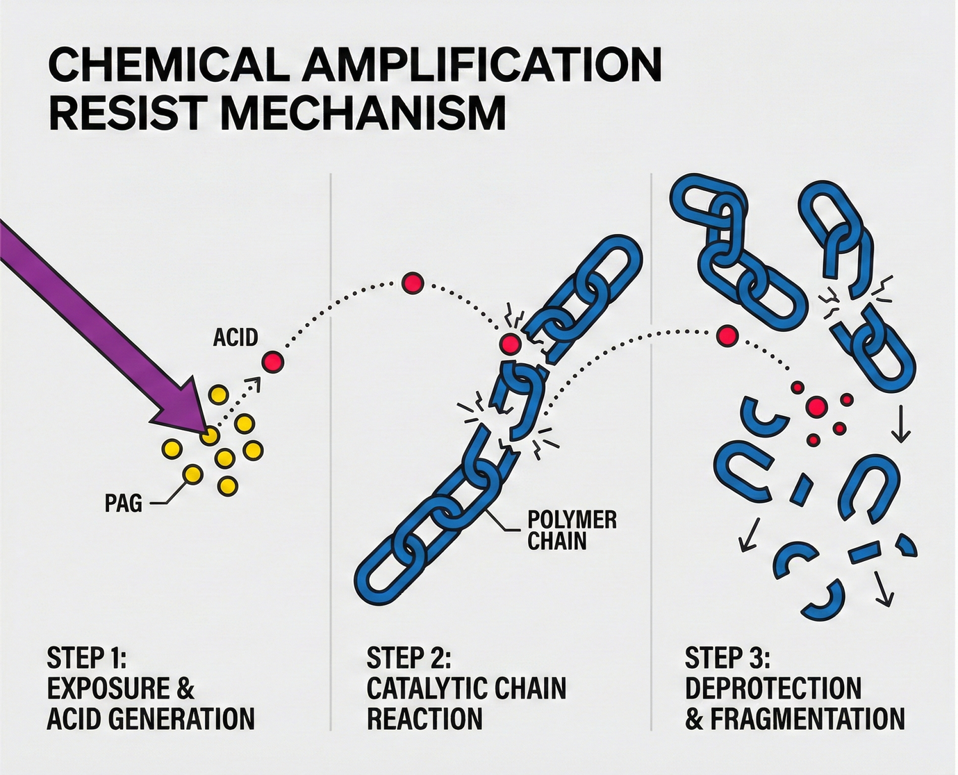
CAR operates on the principle of detonating a nuclear bomb in the microscopic world, triggering a chain reaction. This process is divided into three precise stages:
Stage One: Sniper in Position —— PAG Activation
Photoresist contains a key component called PAG (Photo-Acid Generator). When ASML's EUV photon strikes a PAG, it's like pulling a trigger, causing the PAG to decompose and release a "protonic acid (H+)."
- At this point, the polymer itself has not yet changed; only the "acid" seed has been planted.
Stage Two: The Pac-Man Attack —— PEB (Post Exposure Bake)
This step is when the magic happens. The wafer is placed on a hot plate for PEB (Post Exposure Bake). Driven by thermal energy, the newly generated "acid (H+)" gains kinetic energy and begins to move rapidly through the polymer matrix.
- Catalyst effect: This acid acts like "Pac-man" in a video game. It attacks the protection groups on the polymer side chains, initiating a "de-protection reaction."
- Chain amplification: What's most remarkable is that after cleaving one chemical bond, the acid "does not disappear"; it remains active and proceeds to attack the next molecule.
- Amplification factor: The acid generated by a single photon can cleave hundreds or even thousands of chemical bonds. This is the essence of "chemical amplification" – we use chemical energy (the acid's chain reaction) to compensate for the lack of optical energy (photon quantity).
Stage Three: Police Intervention —— Quencher (Basic Quencher)
If the acid were allowed to diffuse indefinitely, the image would blur. We need someone to call "cut." This is the role of the Quencher (basic quencher), which is typically an amine-based substance.
- Acid-base neutralization: When the acid diffuses to the boundary we've set, it encounters the Quencher. Acid-base neutralization occurs, the acid is eliminated, and the reaction stops.
- Boundary definition: This frontline, where acid and base engage, ultimately defines the edge of the circuit pattern.
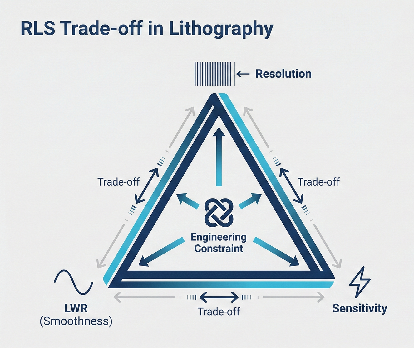
📐 Chapter Two: The Impossible Triangle (The RLS Trade-off) —— EUV's Physical Nightmare
Although CAR technology saved Moore's Law for three decades, by the 3nm (EUV) generation, it hit a wall named physics. This is the renowned RLS Trade-off.
Imagine a triangle with three vertices, representing:
- R (Resolution): How fine can the lines be drawn?
- L (LWR - Line Width Roughness): How smooth are the line edges?
- S (Sensitivity): How fast is the photosensitivity (how high is the throughput)?
In the microscopic world, these three wishes cannot be simultaneously achieved.
1. The Tension of the Triangle
- High Resolution (R): Photoresist molecules must be very small, and acid diffusion distance must be very short (cannot spread too far and blur).
- High Throughput (S): We want photoresist to be extremely sensitive to light, which requires enhancing acid diffusion capabilities (making Pac-man run faster and cleave more).
- Contradiction: Faster acid diffusion (S up) leads to poorer resolution (R down).
- Smooth Edges (L): This is the most difficult. To achieve neat line edges, we need a large number of photons to fill every corner (statistical principle). This implies low photosensitivity and long exposure times.
- Contradiction: Long exposure times lead to a collapse in throughput (S down).
2. Physical Limits: Photon Stochasticity and Shot Noise
Why is EUV so challenging? The culprit is "Shot Noise."
Layman's Analogy: Downpour vs. Drizzle
- DUV (193nm): Photon energy is low, but the quantity is enormous. It's like a downpour. The surface (photoresist) instantly gets fully wet, with a clear water line at the edge.
- EUV (13.5nm): Photon energy is extremely high (14 times that of DUV), but for the same energy, the number of photons is only 1/14 of DUV. This is like a drizzle.
- When we want to draw a 3nm line, the number of falling photons might only be a few dozen.
- These photons fall "randomly (stochastically)." Some areas get 5 photons, while others only get 2.
Result: Dog-Chewed Edges (LWR) Due to the randomness of photon landing points, coupled with the randomness of acid diffusion, the developed circuit edges are no longer straight lines but rather jagged, like they've been chewed by a dog. In the 3nm process, if this jagged error is too large, it can directly lead to two circuit lines bridging (short circuit) or opening (open circuit).
3. Materials Revolution: The Birth of Metal Oxide Resist (MOR)
Traditional organic photoresists (CAR) are long-chain polymers composed of carbon, hydrogen, and oxygen, with large molecular weights and poor EUV absorption capability (carbon atoms do not absorb EUV well). To break the RLS triangle, Japanese manufacturer JSR's subsidiary Inpria proposed a radical idea: "Change the backbone of the photoresist from plastic (carbon) to metal!"
This is the Metal Oxide Resist (MOR).
- Composition: Nanoclusters with a core of Tin or Hafnium.
- Advantage 1 (Super-strong absorption): Tin atoms have an EUV absorption cross-section 4-5 times that of carbon atoms. This means it can capture more scarce EUV photons, addressing the sensitivity (S) issue.
- Advantage 2 (Extremely small molecules): MOR is not a long-chain polymer but tiny nanoparticles. This significantly improves resolution (R) and reduces line width roughness (L).
This was a "dimension-reducing strike" in materials science. It brought a glimmer of hope for Moore's Law below 2nm and established JSR, which controls this technology, as a dominant force that the global semiconductor industry must reckon with.
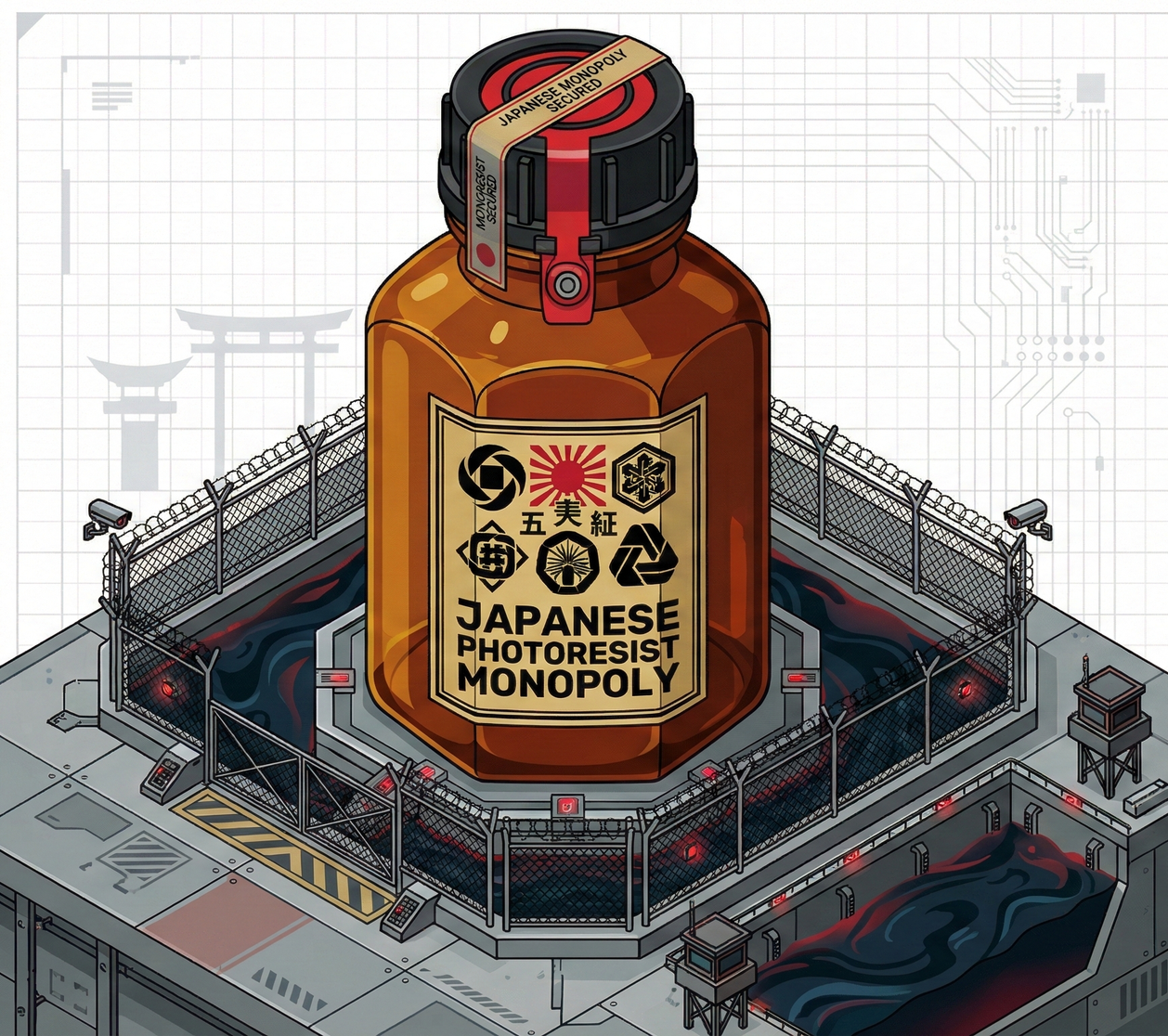
🏯 Chapter Three: The Five Generals of the Japanese Empire (The Big Five)
If ASML holds dominion over "light," then Japan controls the lifeline of "shadows."
The global photoresist market is a suffocating oligopoly. Over 90% of the market share is firmly controlled by five Japanese companies: JSR, Tokyo Ohka Kogyo (TOK), Shin-Etsu Chemical, Sumitomo Chemical, and Fujifilm. This is the deepest and widest moat that Japan's chemical industry has built in the semiconductor sector since World War II. Even powerful players like the United States (Dow Chemical) can only get a slice of the pie in mature processes; in the absolute deep waters of EUV, it is a Japanese solo act.
1. JSR (JSR Corporation) —— The Imperial Army Taken Over by the State
If there is a "jewel in the crown" in the semiconductor materials industry, it is undoubtedly JSR.
- Status: Global leader in photoresists, holding the largest market share in EUV photoresist.
- Key technology: It is the owner of the aforementioned Metal Oxide Resist (MOR) (through the acquisition of US-based Inpria). This means that if you want to produce chips below 2nm, you cannot bypass JSR.
Major Event in 2023: JSR Privatization In June 2023, JIC (Japan Investment Corporation), led by the Japanese government, announced its acquisition of JSR for approximately JPY 1 trillion at a premium, taking it private and delisting it.
- Interpretation: This is extremely rare in capital markets. Privatization is usually for restructuring struggling companies, but JSR is a highly profitable golden goose. Why?
- National Strategy: The Japanese government foresaw future crises. Photoresist development cycles are long and require significant investment, and public companies face short-term financial reporting pressures. To enable JSR to invest in next-generation materials research (such as MOR) without reservation, and to ensure this technology is never maliciously acquired by foreign capital (even allies), the Japanese government decided to directly "nationalize" it.
- Subtext: This is Japan's strongest leverage in the US-China-Taiwan semiconductor rivalry.
2. TOK (Tokyo Ohka Kogyo) —— The Vanguard of Technical Expertise
Compared to JSR's dominance, TOK is more like an ultimate craftsman.
- Distinction: They are one of the very few global manufacturers that have participated in every process, from G-line (micrometer-scale) all the way to EUV (nanometer-scale).
- Relationship with TSMC: TOK is one of TSMC's closest allies. They operate state-of-the-art production lines in Taiwan (Miaoli's Tongluo, Yunlin). When TSMC needs to "fine-tune" a recipe for a specific process, TOK engineers are often the first to rush into the cleanroom.
3. Shin-Etsu (Shin-Etsu Chemical) —— The Unshakeable Giant
Shin-Etsu Chemical is a "titan" in the semiconductor materials industry. It is not only the third-largest photoresist supplier but also the global leader in silicon wafers.
- Strategy: Bundling. Shin-Etsu's sales representatives can tell wafer fabs: "Your latest 3nm process requires our highest-grade silicon wafers, right? Why not also try our photoresist? They work together for even better yield."
- Resilience: This cross-product line integration capability gives Shin-Etsu extremely strong supply chain resilience and pricing power.
4. Sumitomo (Sumitomo Chemical) & Fujifilm (Fujifilm)
- Sumitomo Chemical: Extremely strong in ArF (immersion lithography) photoresists, which are the mainstays of current mature processes (e.g., 28nm, 40nm).
- Fujifilm: Besides photoresists, they are dominant in photoresists for Color Filters. Without Fujifilm's materials, the camera sensor (CIS) in your phone would take black and white pictures.
🇹🇼 Chapter Four: Taiwan's Role —— Agency, Blending, and Breakthrough
At this point, you might ask: "Taiwan has TSMC, so why can't it produce photoresist?" This highlights a brutal gap between "basic science" and "applied engineering."
1. Current Status: Agents and Blending
Currently, most listed companies in Taiwan that are involved in the photoresist sector act as either agents or downstream processors.
- Topco (5434): Taiwan's largest semiconductor materials agent, primarily distributing products from Shin-Etsu Chemical.
- Wah Lee (3010): Another major agent, primarily distributing products from JSR.
- Investment Logic: As long as TSMC operates at full capacity, these agents can effortlessly earn service fees. They are the logistics support for Taiwan's semiconductor industry.
Core Technology Difference: Mother Liquor vs. Blending
- Japanese original manufacturers: They possess the synthesis technology for "mother liquor." This involves synthesizing those special photosensitive polymers from petrochemical raw materials. This is true black technology, with recipes locked in a safe.
- Localization in Taiwan (G-Grade): What TOK Taiwan or Shin-Etsu Taiwan primarily do is "blending and bottling."
- High-concentration mother liquor is shipped from Japan.
- In factories in Taiwan, solvents are added for dilution, viscosity is adjusted, and impurities are filtered out.
- The product is then filled into special brown bottles and delivered to TSMC.
- Value: This is still very valuable (due to timeliness and customization), but the core IP remains in Japan.
2. Breakthrough: Challenging the Impossible —— New Materials (4749)
Amidst the suffocating patent web cast by Japan, one company in Taiwan has torn open a gap: New Materials.
- Strategy: Avoid the main EUV battlefield, opting for a flank attack. New Materials was not foolish enough to directly challenge JSR's EUV photoresist (which requires decades of polymer chemistry accumulation). Instead, they chose to enter the market for specialized process photoresists.
- Achievements:
- CIS (Image Sensor) Photoresist: Successfully entered TSMC's supply chain.
- Micro-LED Photoresist: This is a future display technology, and New Materials has made deep inroads here.
- Significance: This is one of the very few specialty chemical companies in Taiwan that has managed to transition from being an "agent" to an "original manufacturer with R&D capabilities." Although still far from EUV, this signifies that Taiwan is finally beginning to establish its own "formula ownership."
Conclusion: The Choked Throat
2019's Lesson: When Chemicals Become Weapons
In July 2019, the Japan-South Korea trade dispute erupted. The Japanese government announced restrictions on the export of three critical semiconductor materials to South Korea:
- Fluorinated Polyimide
- High Purity Hydrogen Fluoride
- Photoresist
These three items alone (especially photoresist) sent South Korean semiconductor giants Samsung and SK Hynix into a panic, to the point where Samsung Chairman Lee Jae-yong had to personally fly to Japan to "request materials."
Strategic Summary
This incident delivered a profound lesson to the world: In the grand narrative of semiconductors, we often focus on multi-billion-dollar wafer fabs and hundreds-of-million-dollar lithography machines. However, the lifeline of the entire industry might just be that bottle of chemical liquid costing a few hundred dollars.
Photoresist is not merely a consumable. It is a strategic material of nuclear deterrence level. It is Japan's confidence in this digital age, allowing it to "choke the world" even after losing the home appliance and mobile phone markets.
For Taiwan, while we possess the strongest manufacturing capabilities (TSMC), we still rely on others in the puzzle of materials science. This is why the rise of companies like New Materials and Crystalwise Technology holds such critical strategic significance for Taiwan's semiconductor independence.
In-depth Research · Quantitative Perspective
Want to gain more insights into semiconductor quantitative research?
【Insight Subscription Plan】Say Goodbye to Retail Investor Mentality: Build Your Alpha Trading System with 'Quantitative Chips' and 'Consensus Data'EDGE Semiconductor Research
📍 Series Map — Navigate the Complete EDGE Semiconductor Research →


