Preface: The Invisible Obsession with Cleanliness
We often focus on the brilliant laser beam of ASML lithography machines or the violent plasma in etching equipment. However, behind these high-profile moments, the most frequent action in a wafer fab is actually "taking a bath."
- A chip typically undergoes 500–800 steps from silicon wafer to final packaging.
- Of these, 30%–40% are various cleaning and wet etching processes.
- Industry saying: "Wafers are either being etched or on their way to be cleaned."
Why so many cleaning steps? Because in the nanoscale world, the definition of "clean" is completely redefined.
1. Redefining "Purity": PPT (Parts Per Trillion)
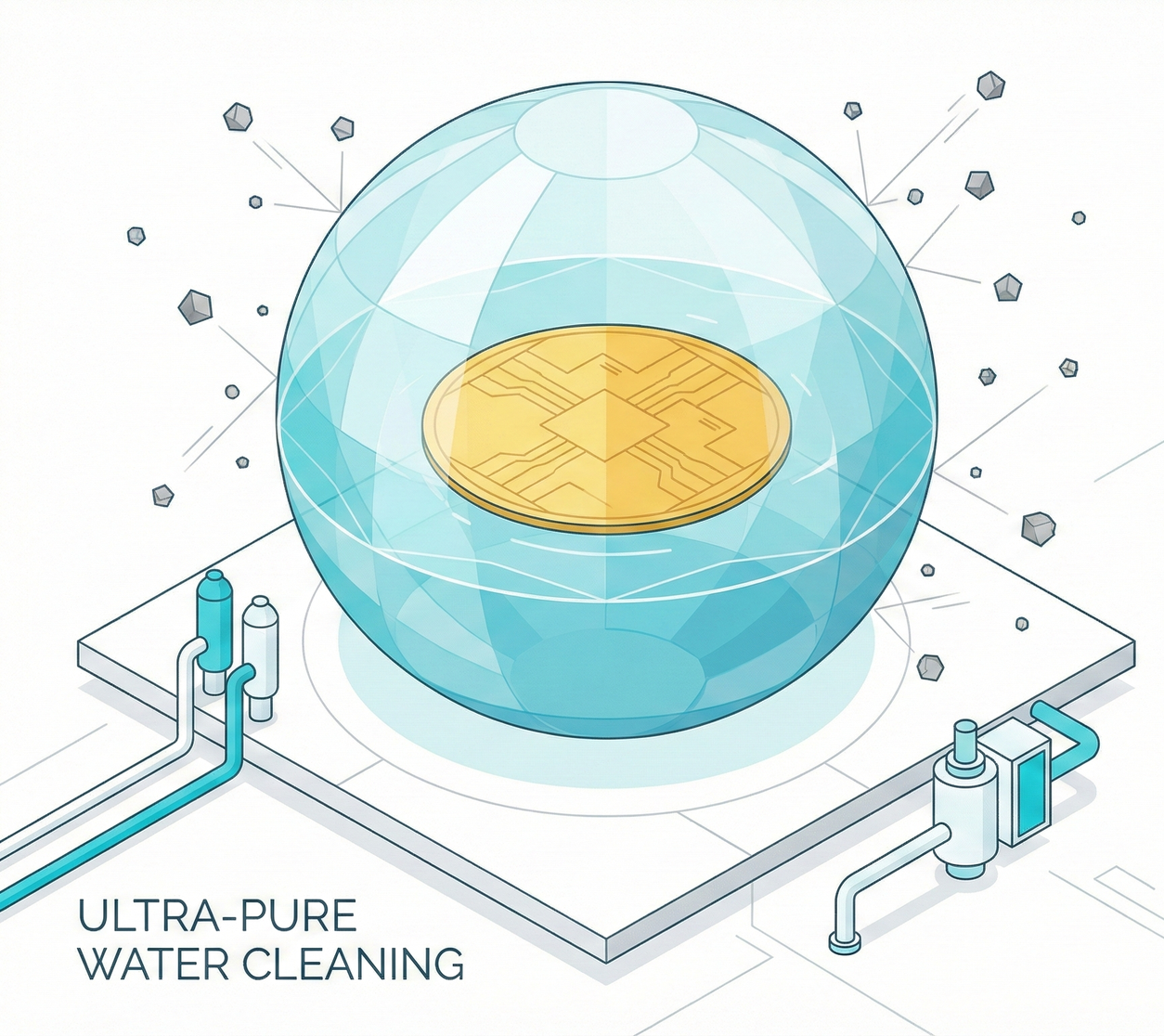
In general industries (food, steel), 99.9% (3N) purity is already considered high quality. But in TSMC's 3nm fabs, this level of purity is almost equivalent to "garbage." Semiconductor chemicals require a purity of PPT (Parts Per Trillion).
To visualize this "counter-intuitive obsession with cleanliness," consider two analogies:
- Olympic Pool Analogy: Imagine 20 standard Olympic swimming pools filled with water. If just one drop of whiskey is added, instruments can still detect it—that's PPT level.
- Coin Analogy: This is equivalent to finding a specific one-dollar coin on the entire surface of the Earth.
If metal ions (sodium, iron, copper) in the chemicals slightly exceed the limit—even by a mere one-hundred-billionth—these conductive ions could penetrate the transistor's gate oxide layer, causing leakage and rendering the entire wafer scrap.
2. Deadly Killers: Killer Particles
Besides chemical impurities, another major enemy is particles.
- 28nm Era: 50nm dust was like small pebbles on the roadside; the circuit might still be able to bypass it.
- 3nm Era: Circuit width is only a few dozen atoms. A 10nm particle (smaller than a virus) is like a giant rock falling in the middle of a highway.
The result is usually:
- Open or short circuits
- Directly crippling the yield
The mission of the wet process is to remove these "giant rocks" one by one amidst the storm of manufacturing processes, maintaining a nearly atomic-level barrenness on the wafer surface.
🧪 Chapter One: The Chemical Task Force (The Wet Chemicals)
Wafer fabs are equipped with a "chemical task force" of diverse personalities. They are not just soapy water, but precisely formulated chemical weapons.
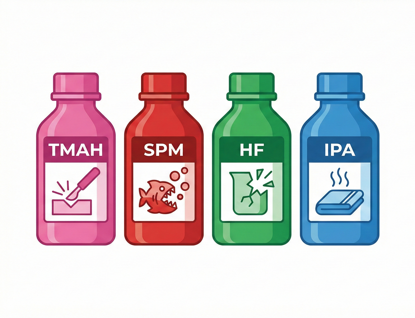
1) Developer —— The Gentle Engraver
- Codename: TMAH (Tetramethylammonium hydroxide)
- Mission: To reveal invisible circuits
After exposure, the photoresist already has a "latent image," but the surface remains flat; TMAH's job is to dissolve the parts that have "softened from light exposure," while not damaging the unexposed areas and not corroding the underlying silicon wafer.
2.39%: Too alkaline, photoresist "walls" are etched away, circuit collapses
2.37%: Too weak, scum remains, subsequent etching fails
Therefore, TMAH not only requires high purity but also absolutely precise ratios, acting as an engraver balancing on the edge of destruction and construction.
2) Piranha Solution (SPM) —— The Ferocious Devourer
- Codename: Piranha Solution (Sulfuric acid + Hydrogen peroxide)
- Mission: To devour all organic life forms
The formula consists of concentrated sulfuric acid ($H_2SO_4$) and hydrogen peroxide ($H_2O_2$). Mixing them causes a violent exothermic reaction, with temperatures instantly soaring above 120°C and boiling. Organic matter remaining on the wafer, such as photoresist residue, fingerprint oils, and dust bacteria, are strongly oxidized and decomposed into carbon dioxide and water, leaving almost "no trace."
3) Hydrofluoric Acid (HF) —— The Cold-Blooded Glass Killer
- Codename: DHF (Diluted HF)
- Mission: To attack the oxide layer
Silicon dioxide ($SiO_2$, essentially glass) is resistant to strong acids and high temperatures, but HF is its nemesis. Silicon wafers naturally form a "native oxide layer" in the air; though only a few angstroms (Å) thick, it can block metal contacts.
Engineers use extremely diluted HF (e.g., 1:100 or even 1:1000) to precisely etch away this oxide layer like a sniper, exposing fresh silicon atoms.
4) IPA (Isopropyl Alcohol) —— The Perfect Towel Utilizing the Marangoni Effect
- Codename: IPA (Isopropyl Alcohol)
- Mission: To "pull" water out
Wafer drying becomes a nightmare at 3nm: water's surface tension is astonishing at the nanoscale. If water gets trapped in high aspect ratio trenches, aggressively spin-drying it can cause Pattern Collapse, like wet paper sticking together irreversibly.
Solution using the Marangoni Effect:
- IPA has lower surface tension than water.
- After spraying IPA vapor, liquid flows from areas of low surface tension to areas of high surface tension.
- IPA penetrates the trenches, dissolves water, and, during evaporation, "pulls" water molecules out one by one like an invisible towel.
This ultimately achieves perfect drying: no water marks and no structural collapse.
🛡️ Chapter Two: The War of Containers —— Topco (4770)'s Teflon Legend
If TSMC is cooking Michelin-starred cuisine, and Japanese manufacturers (JSR, TOK) provide the finest sauces, then the often-overlooked question is: Where should the sauce be stored?
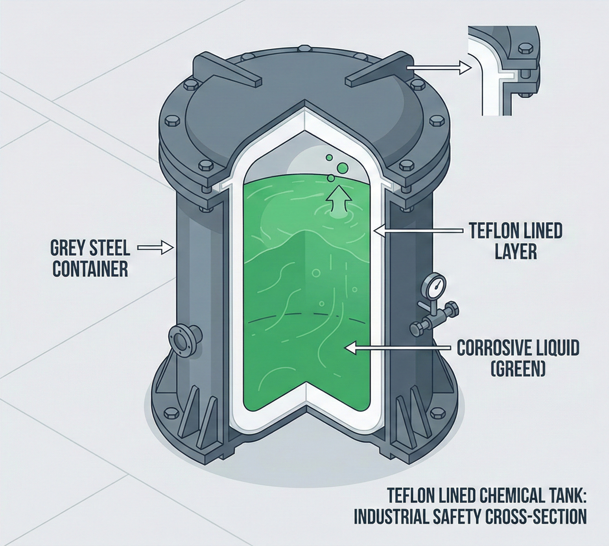
1) Container Paradox: '82 Lafite in a Rusty Tin Can
PPT-grade chemicals are extremely "hungry" and will dissolve any substance they come into contact with:
- Stainless steel drums: Acids will leach Fe/Ni/Cr ions, which are highly toxic to 3nm transistors.
- Ordinary plastic containers (HDPE/PP): May release plastic microparticles or organic additives.
- Glass bottles: HF directly corrodes glass.
Conclusion: A material is needed that is almost immune to all chemicals and is itself extremely pure.
2) King of Materials: PFA's Physical Barrier
The answer is fluoropolymers, commonly known as Teflon (PTFE/PFA).
- The C–F bond is one of the strongest bonds in organic chemistry.
- This gives the material almost invincible chemical inertness: strong acids cannot dissolve it, strong alkalis cannot corrode it, and high temperatures (approx. 200°C) cannot burn it.
- Its surface is extremely smooth with a low coefficient of friction, making it difficult for particles and bacteria to adhere, which is critical for ultra-clean processes.
3) Technical Barrier: How to Stick "Non-Stick" Things?
Teflon is non-stick, so how do you "bond" it to the inside of metal tanks? This is Topco's moat:
- Sheet Lining
- Rotational Molding
If it's just a plastic liner, it can delaminate or blister when subjected to vacuum or drastic temperature changes. Once chemical liquid penetrates the metal interlayer, the tank can corrode from within and perforate, leading to industrial safety disasters.
Topco has mastered the technology of perfectly bonding PFA to the interior of stainless steel tanks, pipelines, and even chemical ISO tanks; the lining must not only resist acids and alkalis but also withstand static electricity and osmotic pressure from high-speed flow of electronic-grade chemicals.
Commercial Status: TSMC's Blood Vessels
After TSMC established fabs in Arizona, USA, and Kumamoto, Japan, the facility chemical systems had to pass the most stringent certifications. Topco followed TSMC overseas, becoming the "vascular doctor" for semiconductor fabs.
♻️ Chapter Three: Developer's Alchemy —— Sanfu Chemical (4755)'s Circular Economy
If Topco solves the problem of "going in clean," then Sanfu Chemical tackles the challenge of "coming out dirty."
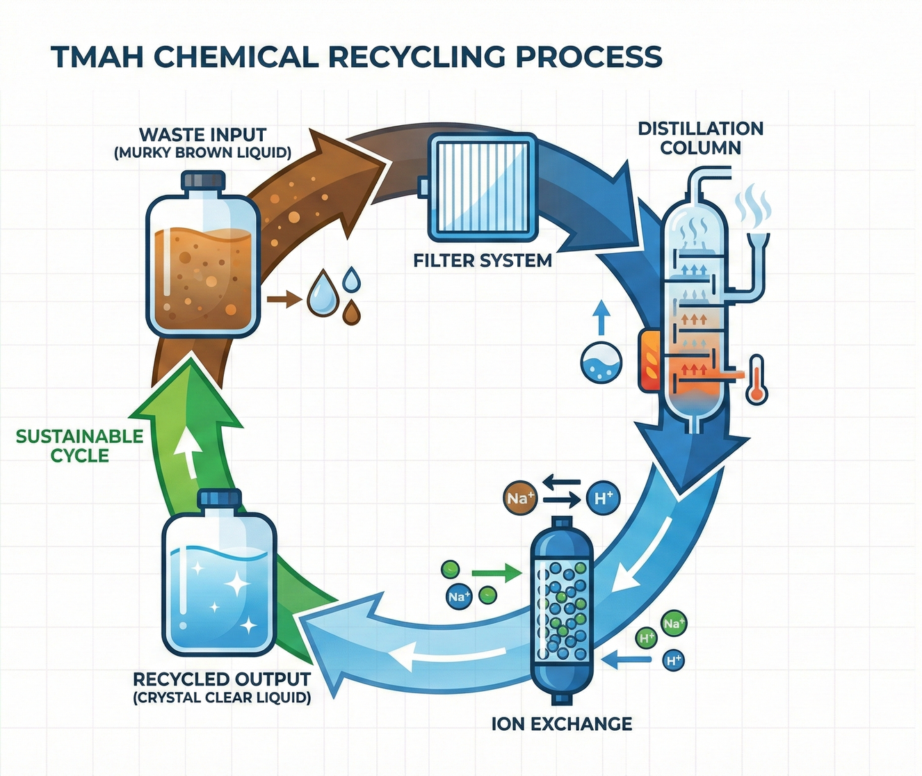
1) Pain Point: The Curse of TMAH
Developer (TMAH) is a strong alkali and biologically toxic (it can damage the nervous system). An advanced wafer fab may consume tens of thousands of tons of TMAH annually.
- Traditional approach: Treat as wastewater, neutralize with acid, then discharge.
- Drawbacks: Buying chemicals costs money, and treating wastewater also costs money.
- Environmental pressure: TSMC faces "Zero Waste" requirements from its supply chain, which is not just a slogan but a prerequisite for orders.
2) Alchemy: Distillation & Purification
Sanfu Chemical developed a "TMAH recovery and purification system," which is not mere filtration but chemical regeneration:
- Collection: Pipelines are routed from the equipment to collect used developer wastewater.
- Electrolysis & Distillation: TMAH is decomposed, and photoresist impurities and water are separated using differences in boiling points.
- Ion Exchange: Special resins are used to adsorb residual metal ions (returning to PPT level).
- Regeneration: The waste liquid is returned to high-purity electronic-grade TMAH (described in the text as 99.9999%).
3) Business Closed Loop: Win-Win
- Free raw materials: Waste liquid has almost zero cost; wafer fabs even pay Sanfu Chemical to handle it.
- High-priced finished product: Purified TMAH is sold back.
- Customer stickiness: The recycling plant is built within the industrial park, sometimes even co-located within the fab (on-site), forming a "fab-within-a-fab" model, making it difficult for competitors to penetrate.
Conclusion: From "Cleaner" to "Gatekeeper"
Looking back at this narrative about wet processes and specialty chemicals, we can see the evolution of Taiwan's role in the semiconductor supply chain:
- Japan is the "Chef": JSR, TOK, and Shin-Etsu hold the most mysterious recipes (photoresists), which represent a 0-to-1 fundamental scientific moat.
- Taiwan is the "Sous Chef" and "Plumber":
- Topco (4770): Ensures molecules remain clean during transport (Teflon lining).
- Sanfu Chemical (4755): Ensures used chemicals can be regenerated (recycling and purification).
In the extreme competition of 3nm and 2nm processes, the decisive factor for yield often lies not in how expensive the lithography machine is, but in whether the water is clean enough and if the pipelines leach impurities. These seemingly insignificant "bathwater" businesses might just be the last line of defense guarding Moore's Law.
For investors, Taiwanese companies with "localized advantages" and a "circular economy moat" are often the most stable shovel and bucket suppliers in a gold rush.
In-depth Research · Quantitative Perspective
Want to gain more quantitative research insights into semiconductors?
【Insight Subscription Plan】Move Beyond Retail Investor Thinking: Build Your Alpha Trading System with "Quantitative Chips" and "Consensus Data"EDGE Semiconductor Research
📍 Series Map — Navigate the Complete EDGE Semiconductor Research →


