In the previous chapter, we witnessed the marvel of the lithography machine: a beam of light passing through a photomask, imprinting patterns of tens of billions of transistors onto a photoresist-coated wafer.
However, remember a crucial physical fact: Photoresist is soft and temporary.
It is merely a layer of polymer. You cannot conduct electricity with polymer, nor can you use it to insulate against current.
Real semiconductor manufacturing only begins at this point.
We must transfer the patterns on the photoresist to 'hard' materials such as silicon, silicon dioxide (insulator), or copper (metal). This requires a violent construction process at the atomic level: digging foundations (etching), pouring concrete (thin film deposition), and leveling the ground (planarization).
In this chapter, we will leave the photolithography area and enter the 'materialization battlefield' monopolized by American and Japanese giants.
I. The Infinite Cycle of Chip Manufacturing
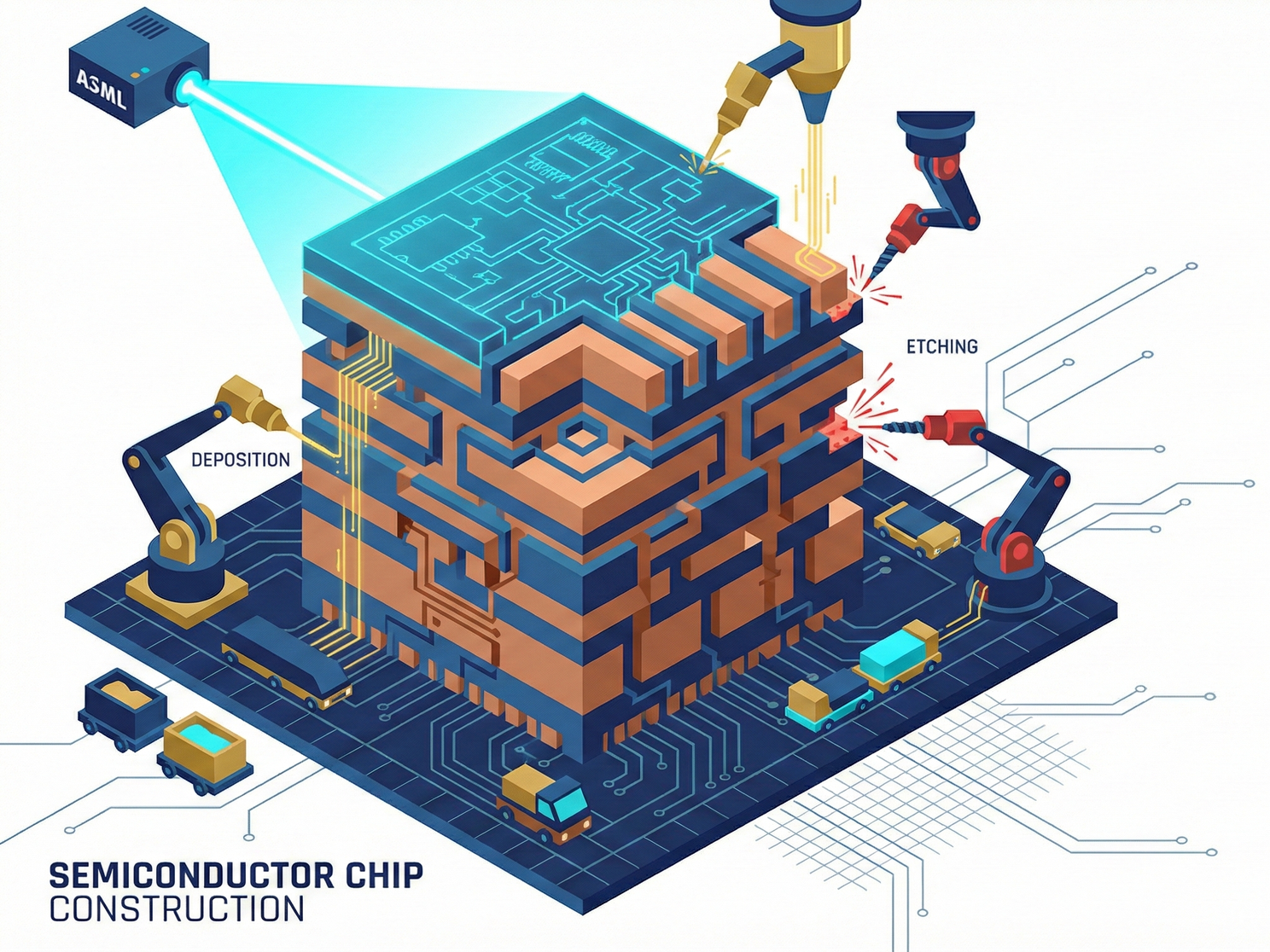
Manufacturing an advanced chip (such as Apple A17 or NVIDIA H100) is like building a 100-story nanoscale skyscraper.
Each floor of this skyscraper (transistor layer, metal interconnect layer, insulation layer) must undergo the same cycle.
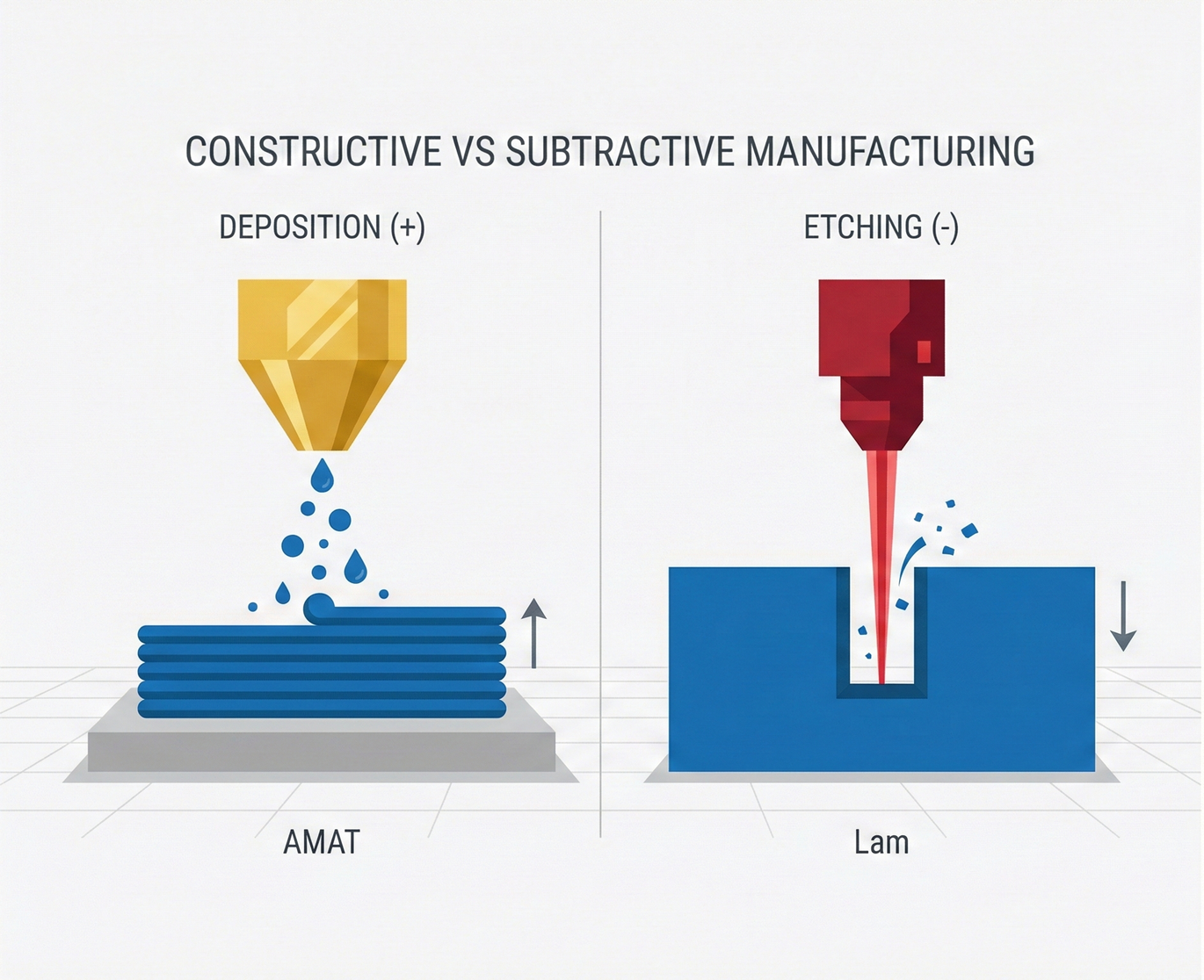
1) Laying the Foundation (Deposition)
- Action: Depositing a layer of material onto the wafer (which could be insulating silicon dioxide, or conductive metals like copper/tungsten).
- Construction Analogy: "Pouring concrete." First, the concrete floor for this layer is laid.
- Dominant Player: Applied Materials (AMAT)
- The global king of "additive processes." If you need to "grow" something new, they are the go-to.
2) Setting up Formwork (Photolithography)
- Action: Coating with photoresist $\rightarrow$ exposure using ASML $\rightarrow$ developing the pattern.
- Construction Analogy: "Setting up wooden formwork."
- On the concrete floor, use wooden boards (photoresist) to create individual frames.
- Areas covered by the boards are to be preserved; uncovered areas will be etched away later.
- Dominant Players:
- ASML: Responsible for drawing lines (exposure).
- TEL (Tokyo Electron): Responsible for applying photoresist and developing the pattern (coater/developer track).
- Note: ASML's machines cannot operate independently; they must be paired with a TEL track.
3) Digging Trenches (Etching)
- Action: Bombarding the wafer surface with strong acids (wet etching) or high-energy plasma (dry etching).
- Construction Analogy: "Drilling and excavating."
- Digging downwards along the areas not covered by the wooden formwork (photoresist).
- This is the most aggressive step: deep wells must be dug without damaging the adjacent formwork or being misaligned.
- Dominant Player: Lam Research
- The "sculptor" of the semiconductor industry. The more advanced the process (e.g., 3D NAND), the deeper the wells dug, and the more Lam earns.
4) Removing Formwork (Stripping & Cleaning)
- Action: Using chemical agents to wash away the deteriorated and spent photoresist.
- Construction Analogy: "Dismantling scaffolding and formwork."
- The wooden boards (photoresist) have completed their task, are removed, and swept away.
- You will see precise trench structures (hard circuits) appearing on the flat concrete surface.
- Dominant Players: TEL (cleaning), Lam Research
5) Leveling the Surface (CMP | Chemical Mechanical Planarization)
- Action: After each layer is built, the surface will inevitably be uneven; if not leveled, the next layer will be built incorrectly.
- Construction Analogy: "Polishing and grinding."
- Using nanoscale sandpaper and chemical slurry to polish the surface mirror-smooth.
- Dominant Player: Applied Materials (AMAT)
- This is also why AMAT's revenue is so high: it handles both "laying the foundation" and "polishing the floor."
6) Troubleshooting (Inspection)
- Action: Using electron microscopes or optical instruments to check for defects such as dust or broken circuits.
- Construction Analogy: "The most meticulous acceptance supervisor."
- If a crack is found on the 10th floor, construction must halt; otherwise, discovering it on the 100th floor would mean wasting the cost of the previous 90 floors.
- Dominant Player: KLA
- The security and insurance company of the semiconductor industry.
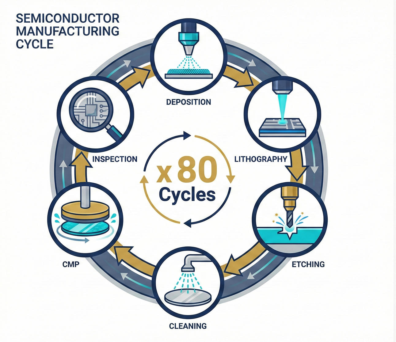
Deposition $\rightarrow$ Photolithography $\rightarrow$ Etching $\rightarrow$ Cleaning $\rightarrow$ Planarization $\rightarrow$ Inspection – these steps form the soul of semiconductor manufacturing.
. While ASML has the highest unit price, it is only responsible for step 2 (photolithography) in the cycle.
. Applied Materials and Lam Research are involved in steps 1, 3, 4, and 5.
. As long as humans are building fabs, a large number of shovels, cement, and cranes will be needed.
II. Applied Materials (AMAT) — The Department Store of the Semiconductor Industry
- Ticker: NASDAQ: AMAT
- Role: The General Contractor
- Keywords: Deposition, Atomic Layer Deposition (ALD), Ion Implantation (Implant)
If only one company could represent the semiconductor equipment industry, it wouldn't be ASML, but Applied Materials (AMAT). It is the world's largest semiconductor equipment manufacturer by revenue (regularly swapping the top spot with ASML).
1) Sells Everything, Strong in Everything
AMAT's strategy is "breadth." Aside from not making lithography machines (that's ASML's territory), it sells equipment for almost every other step.
Need to deposit metal? Call them. Need to planarize? Call them. Need inspection? They have that too.
This gives AMAT extremely strong anti-cyclical capabilities: when memory is weak, it sells logic equipment; when logic is weak, it sells display equipment.
2) Core Moat: Materials Engineering
AMAT's slogan is "We turn silicon into software."
But physically, it is the king of "additive processes": the interconnects (copper), insulating layers (silicon dioxide), and gates (high-k dielectrics) within a chip are all "grown" by AMAT's machines.
- PVD (Physical Vapor Deposition): AMAT's foundational business, with near-monopoly market share. It bombards the wafer with metal atoms using physical impact.
- CMP (Chemical Mechanical Planarization): Planarizes each layer, allowing subsequent layers to be built correctly.
AMAT is the Beta value of the semiconductor industry. As long as humans are building fabs, AMAT will definitely make money.
III. Lam Research (LRCX) — The Artist of Subtraction
- Ticker: NASDAQ: LRCX
- Role: The Precise Sculptor
- Keywords: Etching, 3D NAND
If AMAT is responsible for "creating" materials, Lam Research is responsible for "removing" them. It is the absolute dominant player in global etching equipment.
1) Why is Etching So Difficult?
Imagine digging a deep well in an area the size of a fingernail. This well's depth is 50 times its width (High Aspect Ratio), and its walls must be perfectly vertical, without collapsing or veering off course. This is what Lam Research does every day.
2) Largest Beneficiary of 3D NAND
Lam Research's fate is closely tied to memory (storage).
When NAND Flash transitioned from 2D planar to 3D stacking (from building single-story houses to 200-story skyscrapers), etching demand surged. This is because piercing through 200 layers of material simultaneously requires extremely aggressive plasma etching technology.
Lam Research benefits from technological upgrades. The higher chips are stacked (3D NAND, GAA transistors), the more etching steps are required, and the more Lam earns.
IV. Tokyo Electron (TEL) — ASML's Soulmate
- Ticker: TYO: 8035
- Role: The Track Maker of the Photolithography Area
- Keywords: Coater/Developer, EUV Ecosystem
This is a low-key but formidable Japanese company, and also Asia's largest semiconductor equipment manufacturer.
1) Monopolizing the "Track" in the Photolithography Area
In the yellow room, ASML's lithography machine is always connected to a TEL machine: the "Track" (coater/developer).
- Division of Labor: ASML is responsible for taking photos; TEL is responsible for "loading the film" (applying photoresist) and "developing the photos" (developing).
- Status: TEL has a 100% market share in EUV Tracks. In other words: if TEL doesn't ship, ASML's machines are useless.
2) Does Everything, Second Only to AMAT
Beyond the photolithography area, TEL consistently ranks among the top three globally in etching and thin-film deposition. The Japanese craftsmanship spirit allows them to maintain extremely high yield rates in these precision machinery fields.
TEL is leverage for ASML. If you are bullish on EUV, you must also be bullish on TEL, because every EUV machine requires a Track.
V. KLA (KLAC) — The Inspection Team Specialized in Finding Trouble
- Ticker: NASDAQ: KLAC
- Role: The Expensive Inspector
- Keywords: Inspection, Metrology, Yield
This company is the most "annoying" yet "indispensable" presence in the semiconductor industry. Its gross margin is typically the highest among all equipment manufacturers (consistently >60%).
1) Sells "Fear" and "Insurance"
KLA does not manufacture chips; rather, it "inspects chips."
On a TSMC production line, if a tiny dust particle falls in during the 10th process step but is not discovered, and the subsequent 500 process steps are completed, the wafer is scrapped: you have wasted the electricity, materials, and time for 500 process steps.
KLA's logic is: "Discovering errors earlier saves more money than buying the equipment itself."
2) Data Hegemony
KLA has accumulated decades of defect databases. Even if competitors can build optical microscopes, it is difficult for them to develop algorithms and data feedback loops that can automatically identify "what kind of defect this is."
VI. 2-5-0 Summary: An Oligopolistic Iron Wall
Reading this far, you will discover a striking fact about the semiconductor equipment industry: extreme oligopoly.
- Lithography: ASML (Netherlands)
- Deposition/Planarization: Applied Materials (USA)
- Etching: Lam Research (USA)
- Coating/Developing: TEL (Japan)
- Inspection: KLA (USA)

The most difficult challenge for China in breaking through this blockade is not designing chips (Fabless), or even building factories (Foundry), but rather: if these five companies cease supplying, any advanced process factory would become useless within 24 hours.
In-depth Research · Quantitative Perspective
Want more semiconductor quantitative research insights?
【Insight Subscription Plan】Break Free from Retail Investor Mindset: Build Your Alpha Trading System with "Quantitative Chips" and "Consensus Data"EDGE Semiconductor Research
📍 Series Map — Navigate the Complete EDGE Semiconductor Research →


