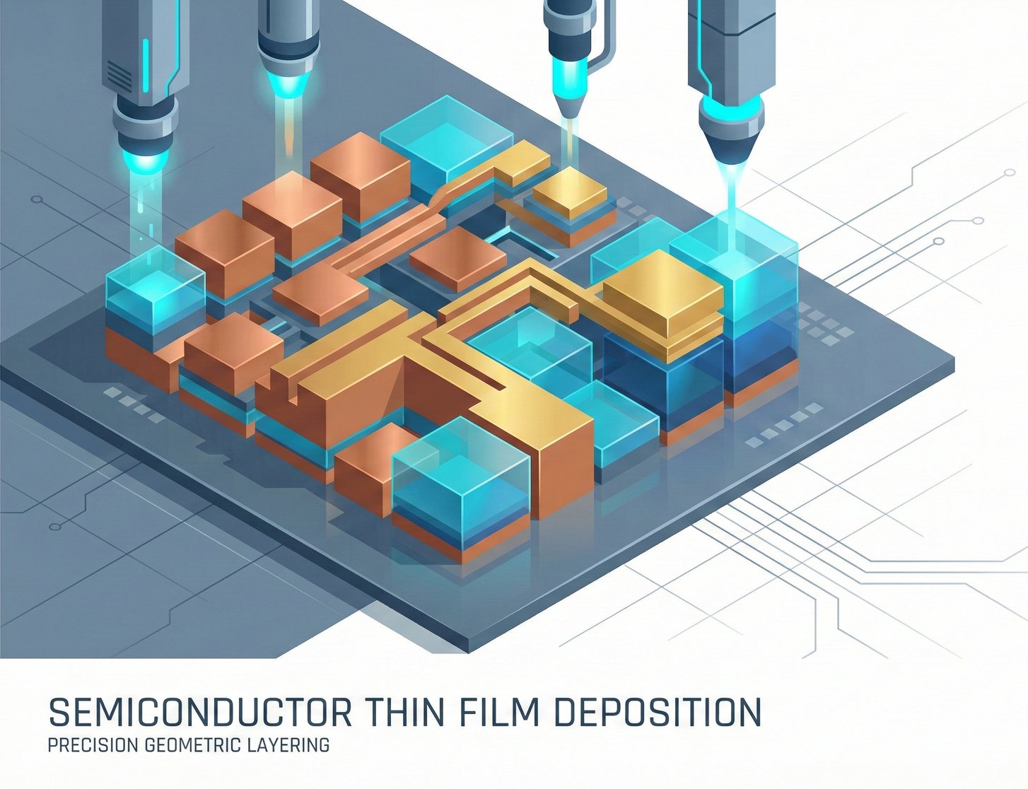
Introduction: The Wafer's Mason
In the chip manufacturing cycle, we need two main types of materials:
- Conductors (Metals): Serving as wires to allow current to pass through (e.g., copper, tungsten, aluminum).
- Insulators (Dielectrics): Serving as walls to separate wires and prevent short circuits (e.g., silicon dioxide, silicon nitride).
The process of "growing" these materials onto wafers is called deposition. Based on different physical principles, it is divided into three major techniques: PVD (Physical Vapor Deposition), CVD (Chemical Vapor Deposition), and ALD (Atomic Layer Deposition).
⚾ Chapter 1: PVD (Physical Vapor Deposition) — The Aggressive Pitcher
Full Name: Physical Vapor DepositionDominant Player: Applied Materials (AMAT)
This is the most intuitive and aggressive additive process. It is typically used for depositing metals.
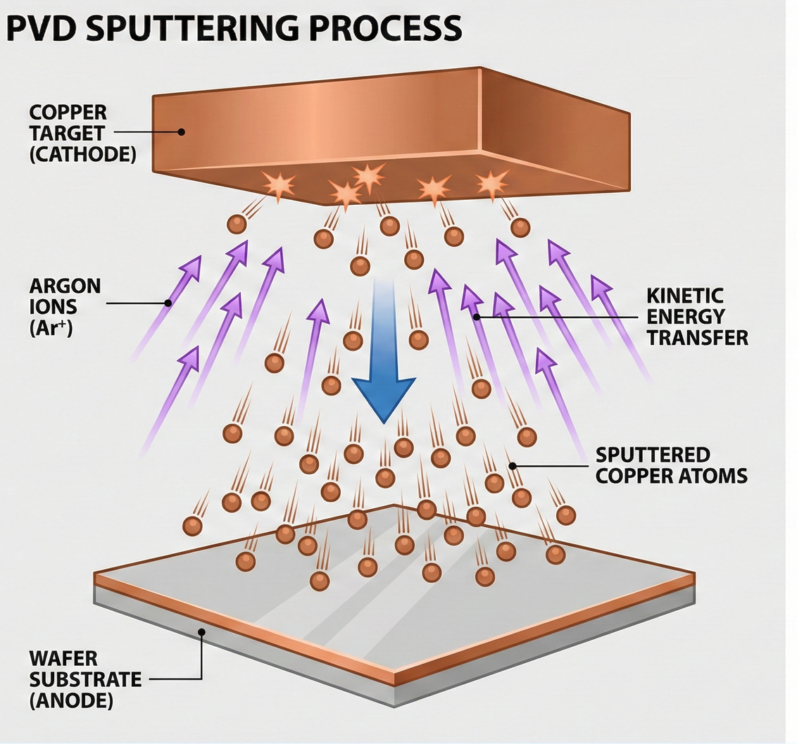
1. Sputtering — The Billiard Ball Principle
- Principle:
- A target material (e.g., a pure copper block) is placed above a vacuum chamber.
- High-energy gas ions (argon gas) are used to strike this copper target.
- Copper atoms are knocked out, falling downwards like bullets, hitting the wafer and accumulating into a thin film.
- Simple Analogy: "Throwing stones in a sandbox."
- The target material is the sandbox, and the ions are the stones.
- If you forcefully throw stones into the sandbox, the sand (copper atoms) will spray out and stick to the adjacent wall (wafer).
- Application: Primarily used for creating interconnects or barrier layers.
- Disadvantage: Because it involves "spraying," the opening (of a narrow feature) tends to accumulate too much material, while the bottom cannot be sprayed. This method is not effective for deep trench (high aspect ratio) structures.
🌨️ Chapter 2: CVD (Chemical Vapor Deposition) — The Gentle Snowmaker
Full Name: Chemical Vapor DepositionDominant Players: Applied Materials, Lam Research, TEL
This involves chemical reactions, not physical impact. It is typically used for depositing insulating layers.
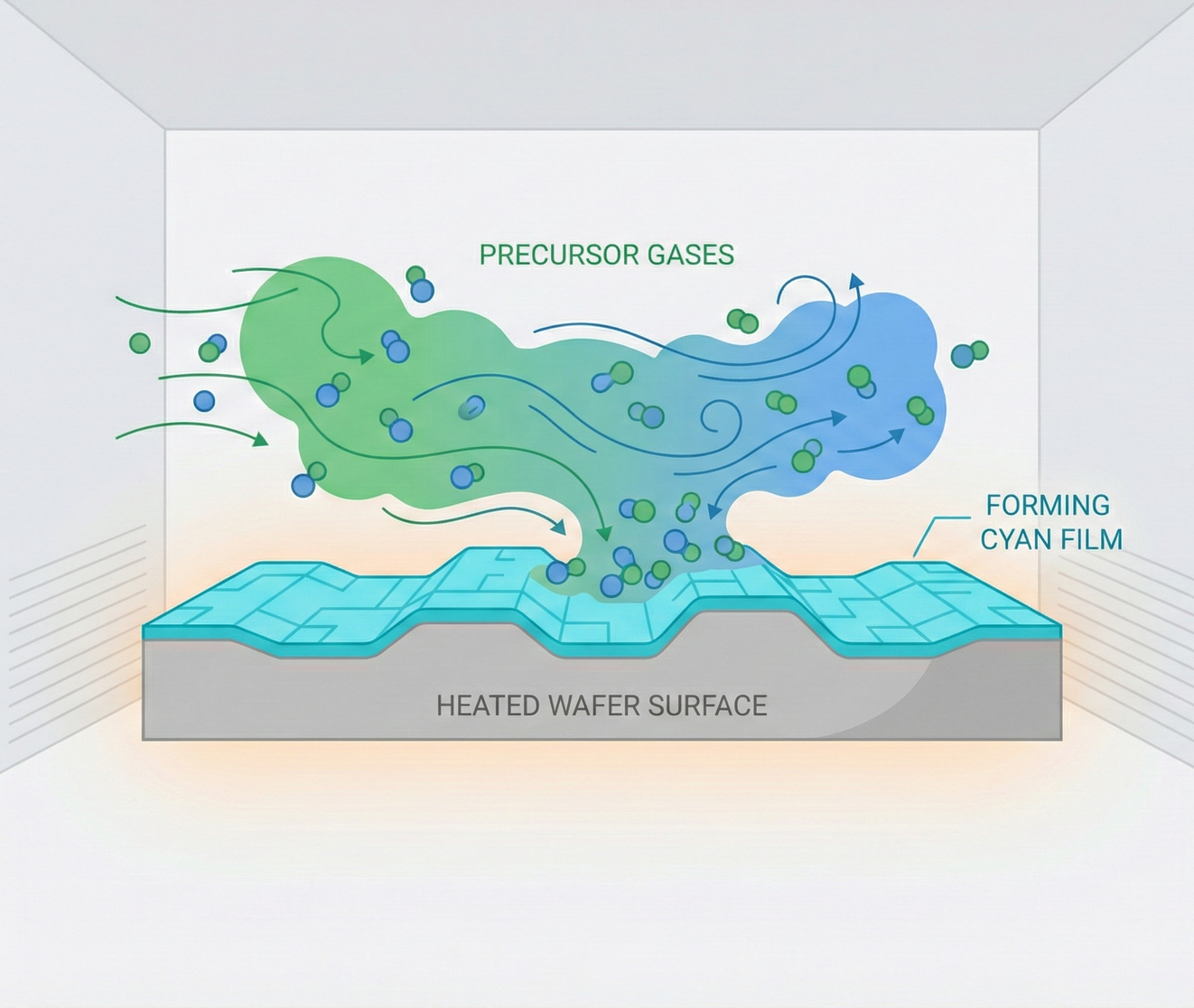
1. Gaseous Reaction — Creation from Nothing
- Principle:
- Two chemical gases (e.g., silane + oxygen) are introduced into a high-temperature furnace tube.
- The gases meet on the wafer surface, undergo a thermochemical reaction, turn into a solid (silicon dioxide), and deposit on the surface.
- Simple Analogy: "Mist in a bathroom."
- Water vapor (gas) in the air encounters a cold mirror, condensing into water droplets (liquid/solid).
- CVD is like a shower of atomic snow on the wafer, where snowflakes uniformly cover the surface.
- Advantage: Offers better coverage than PVD and can penetrate into more complex shapes.
🖨️ Chapter 3: ALD (Atomic Layer Deposition) — The 3nm Savior 🌟 (Most Critical)
Below 7nm, especially for GAA (2nm) structures, traditional PVD and CVD methods become ineffective. Why? Because the features are too small.
- Pinch-off Effect: When using "spraying" (PVD) or "growing" (CVD) methods, the opening of the feature tends to be blocked first, while the inner part of the feature is not yet filled. This creates voids, leading to chip failure.
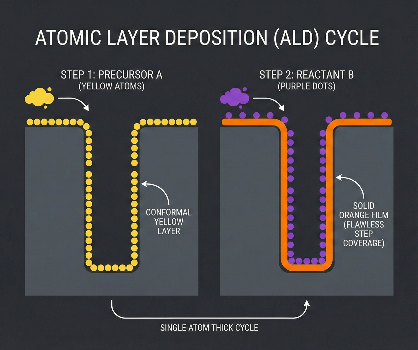
1. ALD's Ingenious Technique — Laying One Atomic Layer at a Time
ALD is the ultimate evolution of CVD. It does not allow gases to enter simultaneously, but rather alternately.
- Steps (The Cycle):
- Inject Gas A: Allow A atoms to adsorb onto the wafer surface (only one layer adsorbs, excess does not stick).
- Purge: Blow away excess A.
- Inject Gas B: Allow B to enter and react with A, forming a thin film.
- Purge: Blow away reaction byproducts.
- Repeat: One cycle completed this way results in a growth of exactly 0.1 nanometers. Want to grow 10 nanometers? Then repeat 100 cycles.
- Simple Analogy: "Velcro" or "Painting."
- Conventional CVD is like pouring a bucket of paint all at once, which often leads to uneven thickness.
- ALD is like a fine brush. Brush a layer, let it dry, then brush another layer.
- Unrivaled Coverage: Even for maze-like GAA structures (where nanosheets are suspended, requiring deposition underneath the sheets), ALD gases can penetrate and uniformly coat every surface with atoms.
2. High-k Metal Gate (HKMG) — ALD's Signature Achievement
- In advanced manufacturing processes, the switch of a transistor (gate) must use a special material called High-k (high-k dielectric material, such as hafnium oxide).
- This material is extremely difficult to process and must be slowly grown using ALD. This is why the stock price of ASM International (ASMI), a Dutch company, has multiplied several times, because it is the leader in ALD.
⚡ Chapter 4: Metallization — The Chip's Vascular Engineering
After depositing the insulating layers and etching the features, we need to fill them with metal for electrical conduction.
1. Challenges of the Copper Interconnect Process
- Copper is an excellent conductor, but it is a "poison". Copper atoms are very active and tend to migrate randomly within silicon, damaging transistors.
- Solution: Barrier Layer
- Before filling with copper, a thin layer of Tantalum or Titanium Nitride must first be deposited using PVD/ALD.
- This is like the lining of a water pipe, preventing copper atoms from permeating.
2. Electrochemical Plating (ECP) — The Gap Filling Expert
- For larger copper interconnects, we do not use PVD (which is too slow); instead, we use Electroplating.
- The wafer is immersed in a copper sulfate solution, an electric current is applied, and copper ions are reduced to copper metal, filling the trenches.
- In this area, Lam Research's Sabre tool is the dominant player.
📊 2-5-1 Strategic Summary: Equipment Suppliers Directory
This table outlines the key players in the deposition sector:
| Technology Area | Core Process | Physical Challenge | Dominant Player (Ticker) | Strategic Importance |
|---|---|---|---|---|
| PVD (Sputtering) | Physical Ejection | Metal interconnects, barrier layers | Applied Materials (AMAT) | The Endura platform is legendary, almost monopolizing the PVD market. |
| CVD (Chemical) | Chemical Film Growth | Insulating layers, rapid growth | AMAT, Lam, TEL | Intense competition, focusing on film quality. |
| ALD (Atomic Layer) | Atomic Layering | GAA structures, High-k materials | ASM International (ASMI), TEL | Fastest growing. Core technology for 2nm process. |
| Electroplating (ECP) | Metal Filling | Copper interconnect filling | Lam Research | Essential for back-end processes. |
Conclusion:
- Applied Materials is the King of Addition: Although ALD faces strong competition, AMAT's position in the PVD and CVD sectors is unshakable. As long as wafer fabs are built, its machines are indispensable.
- ALD is the Diamond of the Future: As chip structures evolve from 2D (planar) to 3D (FinFET) and further to 4D (GAA/stacking), the demand for "uniformity" becomes increasingly stringent. The demand for ALD equipment is increasing exponentially.
Deep Dive · Quantitative Perspective
Want to gain more insights into semiconductor quantitative research?
[Insight Subscription Plan] Bid Farewell to Retail Investor Thinking: Build Your Alpha Trading System with "Quantitative Chips" and "Consensus Data"EDGE Semiconductor Research
📍 Series Map — Navigate the Complete EDGE Semiconductor Research →


