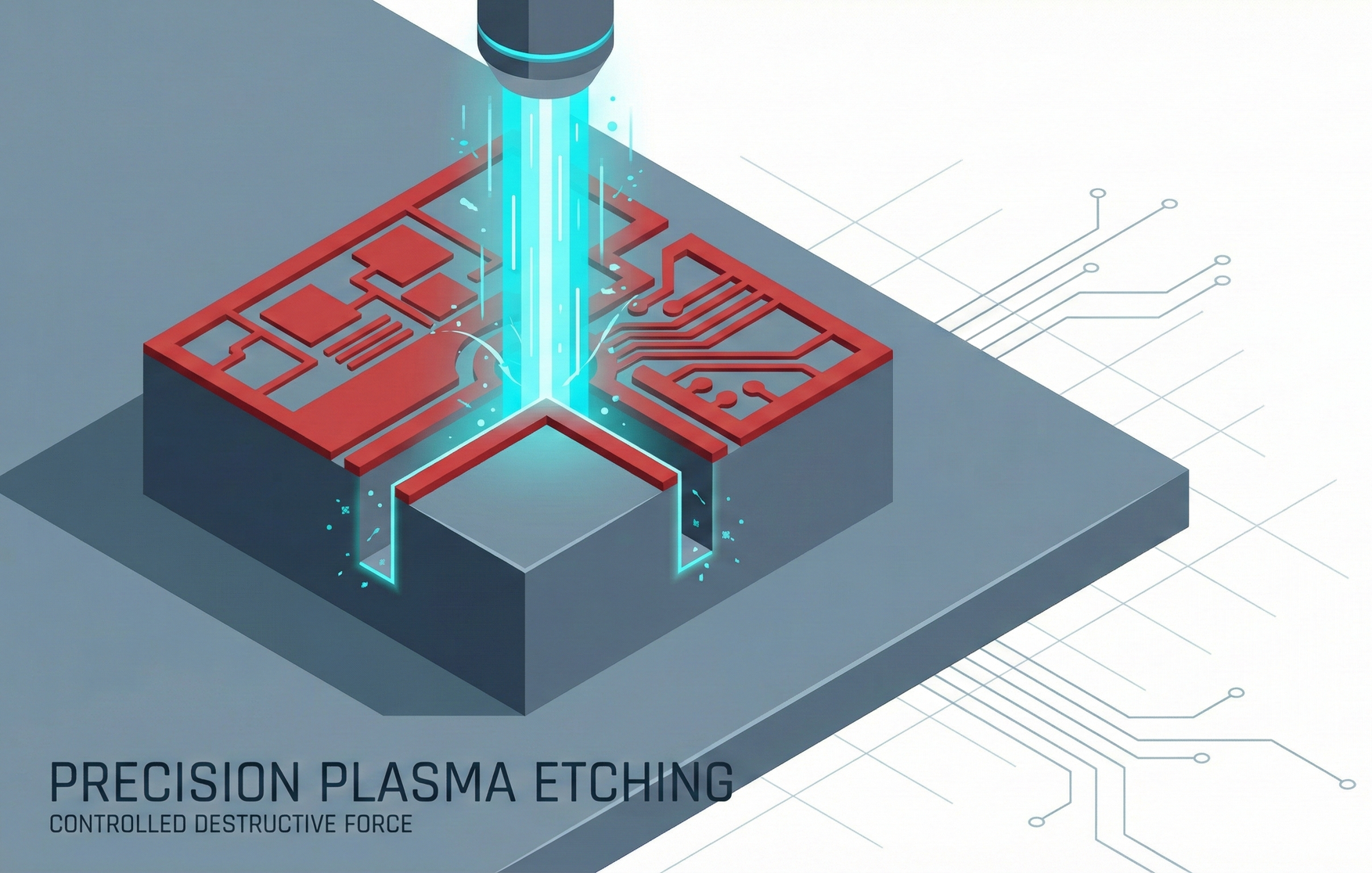
Introduction: The "Destroyer" in the Wafer Fab
The logic of manufacturing chips is counter-intuitive: we first cover the entire wafer with materials (addition), and then remove the unwanted parts (subtraction).
This "removal" process is called etching.
In the semiconductor equipment market, the output value of etching equipment is second only to lithography machines. In this field, one company is the absolute, unshakeable leader – Lam Research.
🔪 Chapter 1: Wet vs. Dry Etching – Bathing or Sandblasting?
Etching is divided into two main types, much like car washing can be "wet wash" or "dry clean".
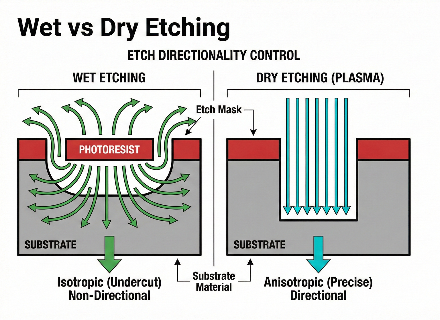
1. Wet Etching – The Gentle Cut of Chemical Solutions
Principle: The wafer is immersed in a strong acid or alkali bath. The solution "dissolves" the areas not protected by photoresist.
Simple Analogy: "A Biscuit Soaking in Milk"
- The solution attacks from all directions (Isotropic)
- Disadvantage: It not only etches downwards but also sideways (Undercut)
- Fatal Flaw: In 3nm processes, lines are already packed closely. If the etching spreads even slightly sideways, two lines will short circuit. Therefore, critical layers in advanced processes absolutely cannot use wet etching.
Application: Removing entire unwanted layers or cleaning the wafer surface.
2. Dry Etching – The Precise Bombardment of Plasma 🌟
Principle: Instead of liquid, it uses gas.
- Gas (e.g., fluorine gas) is introduced into a vacuum chamber, and high voltage is applied, turning it into plasma.
- The plasma is filled with charged, high-energy ions that bombard the wafer vertically like bullets.
Simple Analogy: "High-Pressure Water Jet" or "Sandblasting Machine"
- These ion "bullets" fall vertically (Anisotropic).
- Targeted and precise, only etching downwards, never spreading sideways.
Leader: Lam Research (LRCX)
- This is Lam's moat. It can control the density, direction, and energy of the plasma with atomic-level precision.
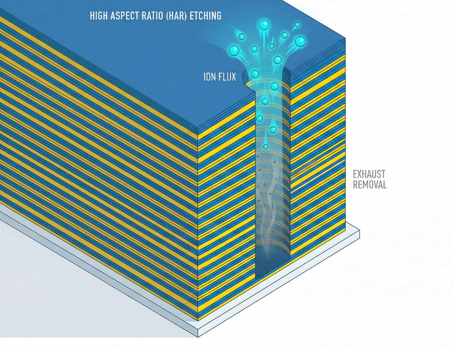
🕳️ Chapter 2: High Aspect Ratio Etch (HAR Etch) – Lam Research's Crown Jewel
This is one of the most challenging problems in semiconductor physics today and a core technology for 3D NAND (memory) and HBM (TSV processes).
1. Physical Challenge: Bottomless Wells
Scenario: 3D NAND is like a 200-story apartment building. We need to drill a hole from the top floor straight to the basement, to be filled with metal as an "elevator".
Data: The depth of this hole is 60 to 100 times its width (Aspect Ratio > 60:1).
Simple Analogy: "Dropping a Stone from the Top Floor of Taipei 101 to the Ground Floor"
- Difficulty 1: The stone (plasma ion) must be thrown accurately without hitting the walls.
- Difficulty 2: The deeper the excavation, the deeper the hole, making it difficult for ions to enter and exhaust gases to escape.
- Difficulty 3: If the drilling goes awry (Tilting), the "building" collapses.
2. Lam Research's Black Tech
Cryogenic Etch: Freezing the wafer to -70°C or even lower. This slows down chemical reactions, protecting the sidewalls from being etched, allowing only the ions at the bottom to continue bombardment.
High-Energy Pulsing: Like a machine gun, plasma is fired in extremely short pulses, forcing ions into the bottom of deep wells.
Strategic Position: The higher the memory stacking layers (176 layers → 232 layers → 300 layers), the better Lam's machines sell. It is the biggest beneficiary of "stacking technology".
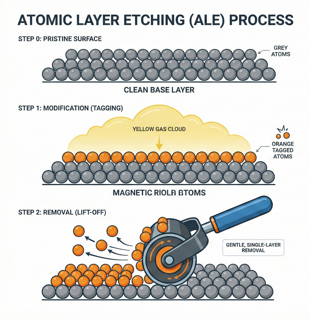
🔬 Chapter 3: Atomic Layer Etching (ALE) – The Surgical Scalpel for 3nm
By the 3nm GAA process, traditional plasma bombardment becomes too aggressive, potentially breaking fragile nanosheets. We need a gentler approach.
1. Technical Principle: ALE (Atomic Layer Etching)
Logic: Instead of removing a large amount at once, I remove only one atomic layer at a time.
Steps:
- Modification: Spray a gas that "modifies" the outermost atomic layer (tags it).
- Removal: Spray another gas or weak plasma to gently remove the "tagged" atoms.
- Cycle: Repeat the above steps.
Simple Analogy: "Lint Roller"
- Conventional etching is like shoveling soil (scooping a large amount at once, easily causing damage).
- ALE is like using a lint roller to pick up dust: rolling it once to pick up a layer, peeling off the sticky sheet, and then rolling again. It's extremely precise and causes no damage to the underlying fabric.
Strategic Significance: This is an essential technology for GAA architecture and 2nm processes. Lam Research and Applied Materials are fiercely competing in this area.
🚿 Chapter 4: Cleaning – The Unsung Hero of CoWoS
After etching, wafers are left with residues and particles everywhere. This is when cleaning equipment comes into play.
1. Wet Process Leaders: TEL (Tokyo Electron) & SCREEN
Japanese manufacturers demonstrate artisan-like dedication to "cleaning".
Single Wafer Clean:
- Previously, a batch of wafers (25 pieces) would be cleaned together. Now, advanced processes clean them one by one.
- High-frequency ultrasonic waves are used to agitate the solution, "vibrating" out contaminants from nano-scale gaps.
2. Opportunities for Taiwan's Supply Chain: CoWoS Packaging Cleaning
Grand Plastic (3131) & Hermes-Epitek (3583)
Why is it important?
- Although advanced packaging (CoWoS) processes are not as fine (micron-level), they generate significant amounts of flux residue and metal debris.
- If not cleaned thoroughly, the chips will short circuit after packaging.
- These two manufacturers in Taiwan, while not involved in 3nm front-end processes, have a very high market share in wet process equipment for backend packaging. They are direct beneficiaries of TSMC's CoWoS capacity expansion.
📊 Strategic Summary: Arms Dealers Directory
This table presents the power map of the etching domain:
| Technology Area | Core Action | Physical Challenge | Leader (Ticker) | Opportunities in Taiwan |
|---|---|---|---|---|
| Dry Etching | Plasma Bombardment | High Aspect Ratio (HAR), etching to the bottom of deep wells | Lam Research (LRCX) (Absolute King), TEL, AMAT | Consumables (Sensei, Kinik) |
| Atomic Layer Etching (ALE) | Layer-by-layer Removal | Precise control of single atomic layers | Lam Research, AMAT | None |
| Wet Cleaning | Chemical Solution Cleaning | Removing nanoscale particles without damaging circuits | SCREEN, TEL (Japanese Monopoly) | Grand Plastic (3131), Hermes-Epitek (3583) (CoWoS-specific) |
| Photoresist Removal | Stripping | Clean and residue-free | Mattson (Chinese-funded), PSK (Korean) | Grand Plastic |
Conclusion
- Lam Research is a winner in vertical growth: As long as memory continues to stack upwards (3D NAND) and transistors become three-dimensional (GAA), Lam's etching machines will be in constant demand.
- Is etching more important than lithography? In some aspects, yes. While EUV is expensive, the number of etching steps is greater. The most numerous machines in a wafer fab are often not from ASML, but Lam's etching machines.
In-depth Research · Quantitative Perspective
Want to gain more semiconductor quantitative research insights?
【Insight Subscription Plan】Break Free from Retail Investor Mentality: Build Your Alpha Trading System with "Quantitative Chips" and "Consensus Data"EDGE Semiconductor Research
📍 Series Map — Navigate the Complete EDGE Semiconductor Research →


