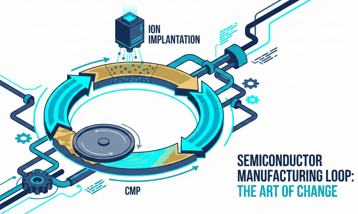
2-5-3 The Art of Change —— Ion Implantation and CMP Planarization
Pure silicon undergoes ion implantation for impurity introduction and thermal annealing for lattice repair. AMAT dominates standard processes; Axcelis monopolizes SiC automotive. CMP planarization flattens wafers, solving photolithography focus issues and is core to CoWoS packaging. AMAT solely d...
Introduction: The Six Cycles of the Microcosm and the "Useless Stone"
Before delving into this power map of semiconductor equipment, we must first establish a "God's-eye view" in our minds.
Chip manufacturing is never a straight line; instead, it's a "Loop" repeated hundreds, even thousands, of times. If you imagine TSMC's cleanroom as a giant skyscraper construction site, the formula for this loop is always:
In previous chapters, we have already examined **addition** (depositing thin films) and **subtraction** (etching trenches). Through these additions and subtractions, we have indeed carved out tens of billions of nanometer-scale 3D structures on silicon wafers.
However, there's a critical physical truth here: **these carved pure silicon structures are essentially "waste."**
Silicon, in its pure state, is an extremely uninteresting element. It neither conducts electricity perfectly like copper nor insulates completely like glass. It's just an unresponsive rock. To transform these rocks into "brains" capable of high-speed computation and precise current switching, we must perform an extremely aggressive "genetic modification" on them.
This is the core of this chapter: **The Art of Change**.
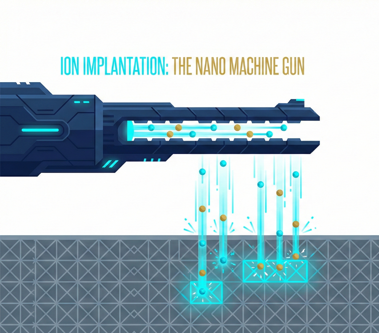
💉 Chapter One: Ion Implantation — The Violent Nanoscale Machine Gun
Semiconductors are called semiconductors because their conductivity is "controllable." The only method of control is called **doping**. In this arena, **Applied Materials (AMAT)** and **Axcelis (ACLS)** hold the power to dictate the physical rules.
1. The Physics of Doping: A Precisely Perfect Cup of Coffee
This is arguably the most magical and fundamental moment in semiconductor physics. We use physical means to forcibly alter the chemical properties of silicon.
Pure silicon has a very stable atomic structure. Each silicon atom has 4 valence electrons, tightly bonded together, leaving no extra electrons to move around, which is why it doesn't conduct electricity.
N-type Semiconductor (Negative): If we forcefully insert a **phosphorus** atom. Phosphorus has 5 electrons; after bonding with silicon, it will have **1 extra free electron**. This additional electron can move freely and carries a negative charge.
P-type Semiconductor (Positive): If we forcefully insert a **boron** atom. Boron only has 3 electrons; after bonding with silicon, it will **lack 1 electron**, forming a "hole." Electrons will scramble to jump into this hole, making it appear as if the hole is moving, carrying a positive charge.
☕
Analogy: The Absolute Domain of Coffee with Sugar Pure silicon is like a premium black coffee, inherently tasteless (non-conductive).
Ion implantation is like adding sugar (phosphorus) or creamer (boron) to it. With sugar, the coffee gains sweetness (acquires conductivity).
However, the terrifying aspect of semiconductors lies in their "abnormal precision." This isn't about adding sugar by feel; it demands precisely dropping "103 grains of sugar" into a standard swimming pool-sized cup of black coffee. One too many, and the chip will leak current and burn out; one too few, and the chip won't function.
2. Ion Implanters: The Earth's Most Precise Particle Accelerators
To embed boron or phosphorus into a rigid silicon lattice, you can't paint it on or soak it in; you must **shoot it in**.
An ion implanter is essentially a small-scale "particle accelerator" (similar in principle to the Large Hadron Collider at CERN or Iron Man's machine for synthesizing new elements in movies).
Its operating logic is full of violent aesthetics:
Ion Source: First, impurity-containing gas is heated and ionized, stripping electrons to turn them into positively charged "ion bullets."
Magnetic Analyzer: This is an ultimate filter. Giant electromagnets are used to bend the ions; impurities that are too heavy or too light will collide with the wall. Only boron or phosphorus ions with precisely the correct weight can pass through the bend.
Accelerator: These bullets are subjected to ultra-high voltages, tens of thousands or even millions of volts, accelerating them to a fraction of the speed of light.
Scanning and Bombardment: These ultra-high-speed bullets, like machine-gun fire, uniformly and relentlessly bombard the silicon wafer, directly penetrating the interior of the silicon atoms.
Here, **voltage determines how deep the bullets penetrate (Depth)**, and **current determines how concentrated the bullets are (Dose)**. Applied Materials (AMAT) has long dominated this market as the leader, thanks to its absolute dominance in high-current and high-energy implanters.
3. The SiC (Silicon Carbide) Curse and the Rise of Axcelis
Understanding the technology allows us to comprehend Wall Street's investment logic. Why has **Axcelis (ACLS)**, a manufacturer of ion implanters, seen its stock price multiply several times in recent years with the explosion of electric vehicles (EVs)?
The answer lies in the physical properties of **third-generation semiconductors — silicon carbide (SiC)**.
Physical Pain Point: SiC is extremely hard (its hardness approaches that of diamond), and its crystal lattice structure is incredibly dense. If you use a traditional AMAT ion implanter on it, either the bullets won't penetrate at all, or the immense impact force will completely destroy the SiC crystal structure, turning it into scrap material.
Axcelis's Unique Expertise: High-Temperature ImplantationAxcelis changed the game. It equipped its machines with an extremely complex heating system, heating the SiC wafer to **above 500°C** while simultaneously firing ions.
🥩
Analogy: The Art of Searing a Steak This is like trying to rub salt (ions) into a piece of raw meat that's just come out of the freezer, hard as a rock; the meat would crack.
Axcelis first sears the steak on a hot plate until it sizzles (high temperature). At this point, the meat's pores open up. When you then sprinkle salt, it perfectly penetrates the meat without damaging its texture.
This technology has given Axcelis a near-monopoly market share in the high-end SiC ion implantation market. As long as the world continues to produce electric vehicles, and as long as car manufacturers need high-voltage fast-charging chips, they must queue up to purchase this "heated machine gun" from Axcelis. This is the best example of technology transforming into a business moat.
🚜 Chapter Two: Annealing — The Phoenix-like Rebirth of the Crystal Lattice
Is the wafer discharged from the hospital after the "injection"? Not yet. It's currently in critical condition.
Because the ion bullets bombarded the wafer with extremely high kinetic energy, the silicon's originally perfectly arranged crystal lattice structure was shattered, becoming a disordered amorphous state. Even worse, the phosphorus or boron atoms forcefully driven in are now merely randomly jammed in the gaps between silicon atoms; they haven't truly "bonded" with the silicon atoms and therefore possess **no conductive function whatsoever**.
We must perform **Thermal Annealing**.
This post is for subscribers only
Sign up now to read the post and get access to the full library of posts for subscribers only.