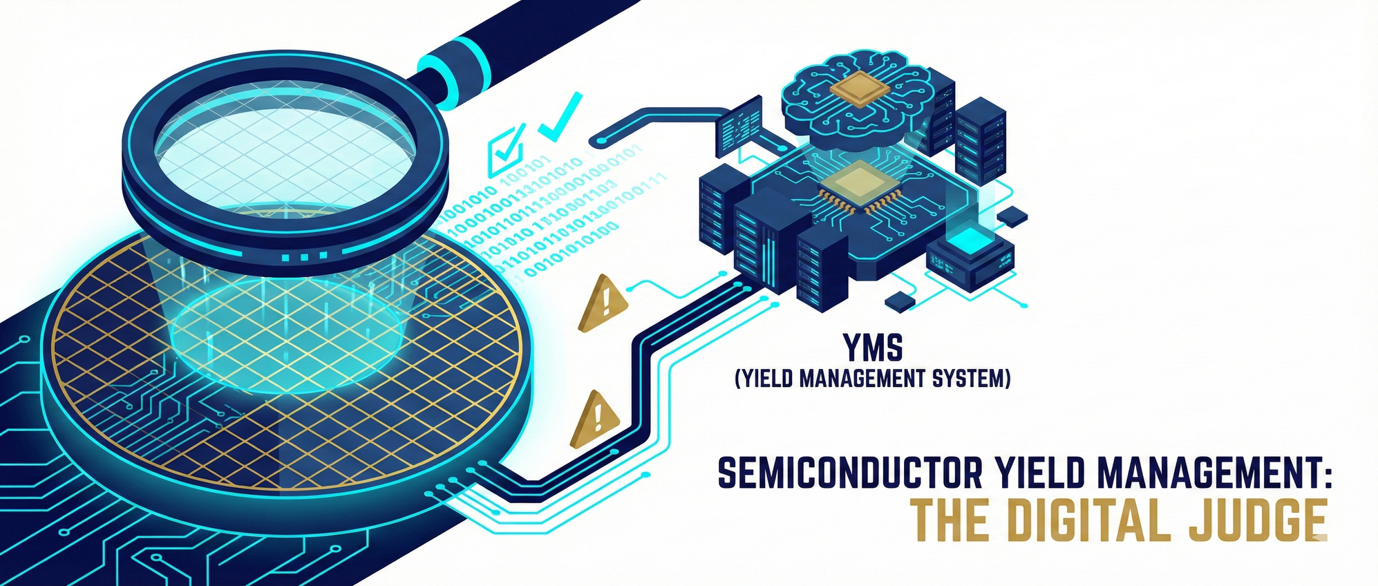
2-5-4 The Art of Quality Control —— Inspection and Metrology
Wafer quality control entails dimension measurement & defect inspection. KLA built deep front-end barriers via its yield database, dominating over 50% market share as 'semiconductor landlord.' CoWoS packaging sparked a back-end inspection revolution, with 3D micro-solder ball inspection demand su...
Preamble: The Six Realms of Reincarnation in the Microscopic World and "Yield Economics"
Esteemed reader, before delving into this chapter, let us once again recall the "God's-eye view" blueprint in our minds.
Chip manufacturing is a vast and unforgiving cycle that permits no margin of error. The formula for constructing this nanometer skyscraper is:
Deposition (laying concrete) $\rightarrow$ Photolithography (drawing blueprints) $\rightarrow$ Etching (digging trenches) $\rightarrow$ Ion Implantation (altering material properties) $\rightarrow$ Planarization (leveling floors) $\rightarrow$ Inspection and Metrology (acceptance and error detection)
We have now completed all the preceding physicalization engineering processes, filled with "brute force" and "magic."
Now, one floor of the building has been constructed, but we face an extremely pragmatic business question:
Can this floor actually be inhabited?
The wafer fab war, in essence, is a war of yield.
Yield 50%: If a wafer fab produces two chips and one is faulty, the massive depreciation and material costs alone will drive you to bankruptcy (this was the dire situation Intel faced when it was stuck at 10nm).
Yield 90%: If only one out of ten chips produced is faulty, the wafer fab will gush out extraordinary profits like a money printer.
And on this razor-thin line between success and failure, there is a "Supreme Court judge" with the power of life and death. It does not produce any chips, is not responsible for etching, nor for stacking.
Its sole value lies in:
Identifying the culprits
Preventing future issues
It can precisely tell TSMC: "That $300 million etcher you just used experienced a slight temperature drift of 0.5 degrees in chamber #3, causing the lines at the edge of the wafer to deviate by 1 nanometer. Shut down immediately, or this batch of wafers, worth tens of millions, will all be scrapped!"
The semiconductor quality control system is strictly divided into two major moats:
Metrology: Measuring if "dimensions" are correct
Inspection: Finding "defects"
📏 Chapter One: Metrology — The Nanometer Tailor's Absolute Ruler
Mission: Measure dimensions.
Core Question:
If an engineer draws a line that is 3 nanometers, is what the machine etches truly exactly 3 nanometers?
In the macroscopic world, we measure length with a ruler.
But in the nanometer world, the laws of physics will play tricks on you.
Metrology equipment must contend with the limits of optics, with precision requirements reaching atomic levels.
1. Critical Dimension (CD) Metrology
Physical Challenge: The Curse of Diffraction
We need to measure an electrical circuit line that is one ten-thousandth the thickness of a human hair.
The wavelength of visible light (approximately 400 to 700 nanometers) is much coarser than the 3-nanometer line you want to observe; light waves will simply "diffract around" it, making imaging impossible.
Solution: CD-SEM (Scanning Electron Microscope)
Since light waves are too long, we switch to an electron beam.
Electrons have extremely short wavelengths, which can easily penetrate physical limits to reveal nanometer-scale fine structures.
CD-SEM precisely delineates the width and depth of trenches by collecting reflected secondary electrons.
Dominant Players: Japan's Hitachi High-Tech and the United States' Applied Materials
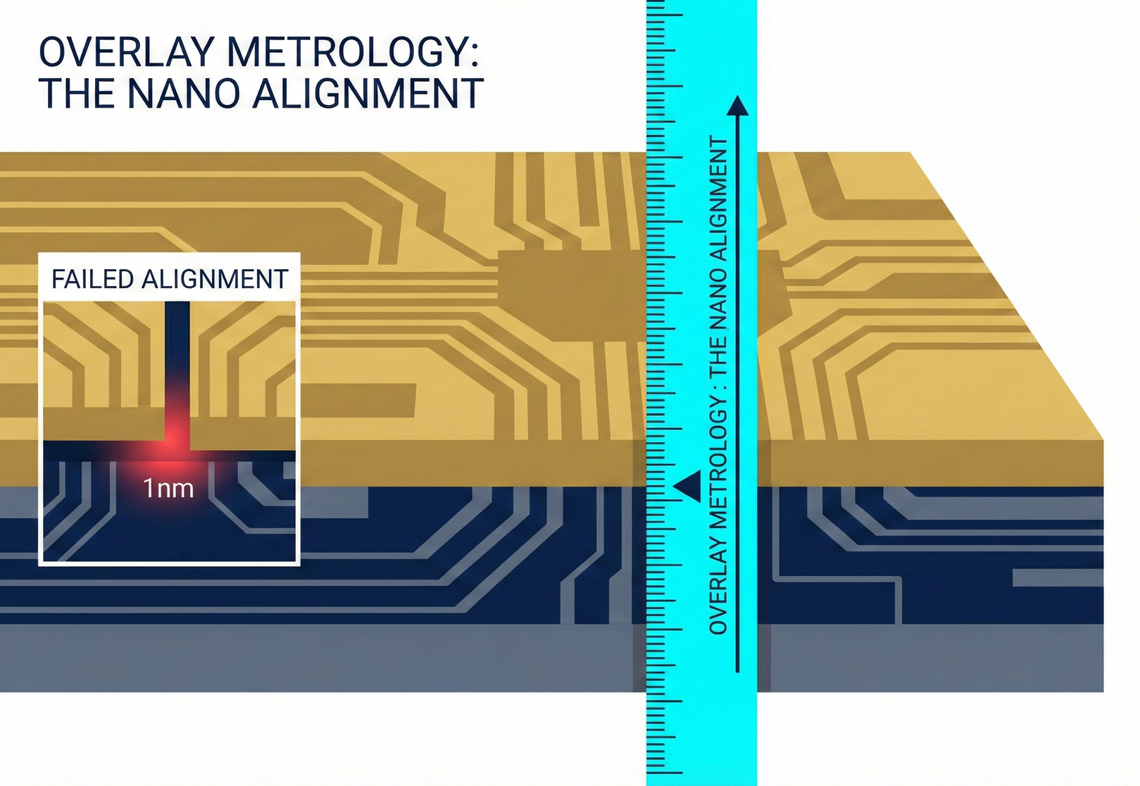
2. Overlay Metrology (Extremely Critical)
This is the most error-prone and fatal step in chip manufacturing.
Physical Scenario: A chip is a 100-story building. The first floor has a foundation, and the second floor needs columns.
Extreme Challenge: The columns on the second floor must "perfectly align" with the foundation on the first floor.
If it deviates by 1 nanometer, the metal interconnects between the upper and lower layers will not connect, resulting in an open circuit.
Layman's Analogy: Nanometer-scale Human Pyramid
Imagine a human pyramid formation with 100 people.
When building up to the 50th person, if a foot deviates even 1 centimeter from the shoulder of the person below, the entire 100-person tower will instantly collapse.
Mission of Overlay Tools: After each layer of photolithography exposure, immediately check for "alignment."
Dominant Players: KLA and ASML
Although ASML's machines are extremely precise, wafers undergo unpredictable physical deformation (warp) after high-temperature baking and CMP planarization.
Therefore, wafer fabs must rely on KLA's Overlay equipment to confirm "whether alignment is achieved" and immediately feedback error data to the lithography machine for correction.
3. Film Thickness Metrology
Mission: Check whether the film deposited by CVD or ALD is perfectly uniform in thickness.
Principle: Ellipsometry
A beam of light with a specific polarization is directed onto the wafer surface.
As the light penetrates the thin film and reflects back from the underlying layer, its polarization state (rotation angle) undergoes distortion.
By analyzing the distortion angle, the film thickness can be calculated inversely.
If metrology is about measuring whether a garment's size is correct, then inspection is about checking whether the garment has "holes or stains."
Mission: Find defects.
Core Question:
Did a speck of dust fall here? Is that line broken? Are these two lines stuck together, causing a short circuit?
Inspection technology in the semiconductor industry is divided into two major schools:
Optical (Extremely Fast)
Electron (Extremely Precise)
The two perfectly complement each other.
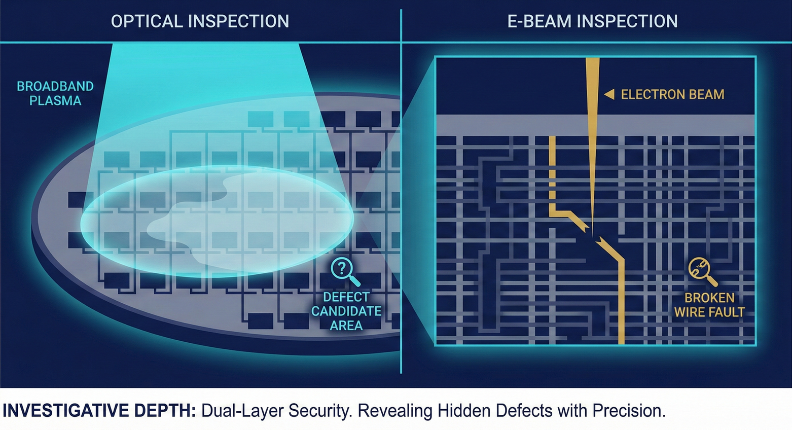
1. Optical Inspection — Satellite Aerial View
Principle: Uses an ultra-strong light source (typically Broadband Plasma) to scan the entire wafer.
Compares the "standard design pattern (Die-to-Database)" with the "actual printed pattern (Die-to-Die)."
If unusual light reflections appear, it indicates "something is wrong" (a defect).
Advantages: Extremely Fast
A full 12-inch wafer can be scanned in minutes.
Like a satellite taking aerial photos of an entire city, instantly identifying congested main roads or buildings on fire.
Disadvantages: Limited Resolution
Due to optical limits, very small (sub-nanometer) defects are unclear, appearing only as a blurry dark shadow.
Dominant Player: KLA (29xx/39xx series)
KLA's broadband plasma optical inspection machine is one of the most expensive non-lithography equipment in TSMC's fabs.
Top-tier optical sensors and algorithms can precisely detect Killer Defects in a vast ocean of data.
2. E-Beam Inspection — The Street View Car with a Magnifying Glass
When an optical inspection machine finds an area that "seems off" but cannot see clearly what it is, an E-Beam inspection machine is called in.
Principle: Abandons optics and uses an electron beam (E-Beam) to slowly and finely scan the wafer surface.
Advantages: Extremely Precise, and possesses "Electrical X-ray Vision"
Not only detects physical defects at the atomic level.
Can also detect electrical defects through "Voltage Contrast."
For example: an area might appear connected visually (optical inspection judges it OK), but an E-beam scan reveals no current flow, proving it is actually broken internally.
Disadvantages: Extremely Slow
Optical inspection is like a satellite aerial photo.
E-Beam is like a Google Street View car.
Scanning an entire wafer can take several days, thus it is typically used for new process R&D debugging or limited sampling in mass production.
Dominant Players: ASML (HMI Hermes Microvision) and Applied Materials
Taiwan's pride, "HMI (Hermes Microvision)," was once the global leader in this field and the top-performing stock on the Taiwan Stock Exchange.
In 2016, it was acquired by ASML for a staggering price of hundreds of billions of New Taiwan Dollars.
This acquisition proved that the strongest lithography machine (ASML) must be tied to the strongest electron eye (HMI) to survive in extreme processes below 3 nanometers.
🏰 Chapter Three: KLA — The Absolute Moat of the Data Empire
In the field of inspection and metrology for semiconductor front-end processes, KLA's global market share has consistently remained at an astonishing 50% or more.
This is an absolute dominion that even equipment giants like Applied Materials and lithography machine titan ASML cannot shake.
Why?
This post is for subscribers only
Sign up now to read the post and get access to the full library of posts for subscribers only.