Before we delve into the life-and-death battle between TSMC and Samsung, we must first understand the nature of the battlefield. Whether it's an NVIDIA H100 chip priced at NT$100,000 or an inexpensive MediaTek chip in your smartphone, if you magnify them tens of thousands of times under an electron microscope, the tens of billions of transistors inside are actually doing only one thing from start to finish: switching electrical current on and off.
The essence of a transistor is a miniature faucet.
It consists of four core components:
- Source: The water tower. This is the inlet for water (electrons).
- Drain: The bucket. This is the outlet for water (electrons).
- Channel: The pipe connecting the Source and Drain, the path water must take.
- Gate: The faucet handle (valve). Apply voltage to it, the valve opens, conducting electricity (signal is 1); no voltage, the valve closes, cutting off electricity (signal is 0).
Semiconductor engineers pursue one ultimate goal throughout their careers: when the Gate (valve) says 'stop,' not even a single drop of water must flow through the Channel (pipe).
🌊 Chapter 1: The Arch-Nemesis —— Short Channel Effect
If it were just about making a faucet, humans perfected it decades ago. Why is it that with advanced manufacturing processes, the faucet suddenly 'cannot be shut off tightly'? Because Moore's Law, with a knife, is forcing engineers to cut the Channel (pipe) shorter and shorter.
- The Golden Age of Long Channels (Older Process Nodes): When the pipe was long (e.g., 90 nm era), the Gate handle had absolute dominance. It stood high above, a gentle press would obediently cut off the water flow in the middle.
- The Collapse Moment of Short Channels (Advanced Process Nodes): When the pipe length was drastically shortened to below 20 nanometers, physics collapsed, and two fatal phenomena occurred:
- Loss of Control: The Source (inlet) and Drain (outlet) are so close that their powerful electric fields start interfering with each other. The Gate, stuck in the middle, is like an ineffective manager, unable to stop the private communication between the two sides even if it shouts itself hoarse.
- Quantum Tunneling: This is the most terrifying. Because of the extremely short distance, electrons transform from physical 'marbles' into 'waves'. They don't need to travel through the channel; they directly become ghosts, 'tunneling' from Source to Drain.
Outcome: Even if you shut the Gate tightly (0), current still stealthily flows through. In physics, this is called 'Leakage Current'. The real-world consequence is that: your phone, though unused in your pocket, feels hot like a hand warmer and runs out of battery in half a day.
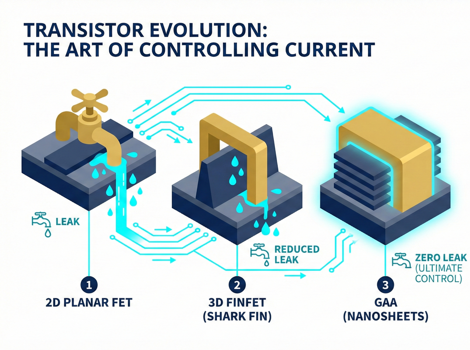
To combat this arch-nemesis, humankind embarked on three generations of transistor structural evolution.
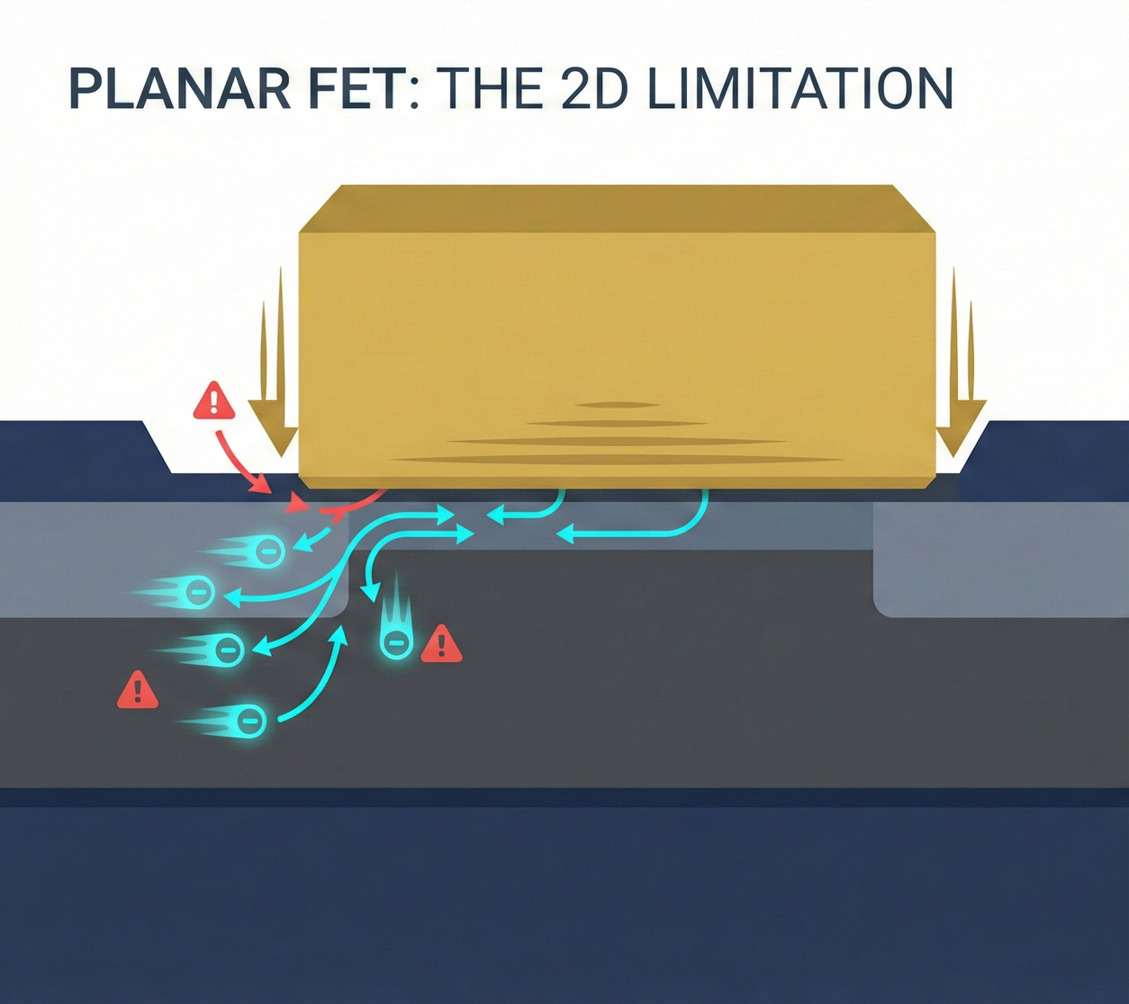
🦶 Chapter 2: Planar FET —— The End of the 20 nm Node
This is the classic structure that dominated the semiconductor industry for decades.
- Structure: 2D planar. The Channel lies flat on the silicon wafer surface, and the Gate, like a slab, presses down from directly above.
- Control Surface: Only 1 surface (top).
💡 Investor's Analogy: Stepping on a Hose Imagine a plastic hose lying on an asphalt road, and you firmly step on it with your foot (the Gate pressing down). When the hose is thick, this method is very effective. But if this hose is partially buried in the soil (meaning the leakage path occurs deep within the silicon substrate), even if you step on it from above, water will still stealthily flow through the gaps in the soil.
Outcome: By the 20 nm node, Planar FETs were officially declared obsolete. No matter how powerful the lithography machine, the leakage current problem could not be solved. Moore's Law was seemingly about to end here.
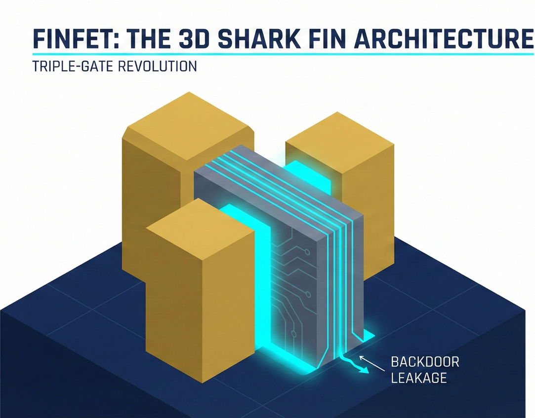
🦈 Chapter 3: FinFET (Fin Field-Effect Transistor) —— The Fin That Saved the World
Just as Moore's Law was about to suffocate, Dr. Chenming Hu, former CTO of TSMC, invented FinFET. This great invention was the core moat that allowed TSMC to completely pull ahead of Samsung and dominate the industry from 16 nm to 3 nm for a full decade.
- Structure: Standing the pipe 'upright'. Since a single surface (from top down) couldn't contain it, engineers simply dug out the flat-lying Channel, making it stand vertically on the substrate, transforming it into a 3D shape resembling a fish's dorsal fin (Fin). Then, the Gate was made into a 'ㄇ'-shaped (U-shaped) clamp, directly straddling the fin.
- Control Surfaces: Increased dramatically to 3 surfaces (left, right, top).
💡 Investor's Analogy: Pinching a Hose with Fingers You're no longer simply stepping on it; you're firmly 'pinching' the hose from three directions with your thumb, index finger, and palm. Control instantly surged! Not only was the leakage problem solved, but because the contact area increased, the drive current strengthened, allowing chips to operate at lower voltages, becoming both faster and more power-efficient.
Why did FinFET also hit a wall at 3 nm?
Given how perfect FinFET seemed, why did TSMC decide to phase it out at 2 nm, and Samsung at 3 nm? Because it faced two insurmountable physical contradictions:
- The Curse of Aspect Ratio: If chip designers wanted greater current (to make the chip compute faster), the fins had to be made 'taller' (to increase contact area). But at the same time, to combat leakage current, the fins had to be made 'extremely thin'. Have you ever tried to build a nanometer-scale wall on flat ground that is tall, thin, and unsupported? It would collapse directly during the manufacturing process.
- The Fatal Backdoor: Although you pinched the left, right, and top surfaces, the 'bottom' of the fin was still connected to the silicon substrate. When the size shrunk to below 3 nm, electrons would escape through this only unpinched 'backdoor' at the bottom.
✊ Chapter 4: GAA (Gate-All-Around) —— The Ultimate Savior for 2 nm
Since the bottom would leak current, let's hollow out the bottom as well! This is the absolute pinnacle of what human physics and engineering can achieve today.
- Structure: Suspending the pipe 'in the air'. Engineers performed incredible magic, completely detaching the Channel from its foundation, suspending it in the air. These Channels were made into several horizontally stacked nanosheets, resembling layers of lasagna stacked on top of each other. Then, the Gate, like cheese, was completely poured into and filled the gaps between each layer of lasagna.
- Control Surfaces: Achieving the ultimate 4 surfaces (top, bottom, left, right, 360-degree coverage).
💡 Investor's Analogy: Firmly Gripping the Hose You are no longer pinching with three fingers; your palm completely, 360 degrees without blind spots, envelops the entire hose. Electrons are completely trapped within the nanosheets, with nowhere to escape. As soon as the Gate gives the 'stop' command, electrons must brake instantly. The leakage current problem has been reduced to the lowest physical limit.
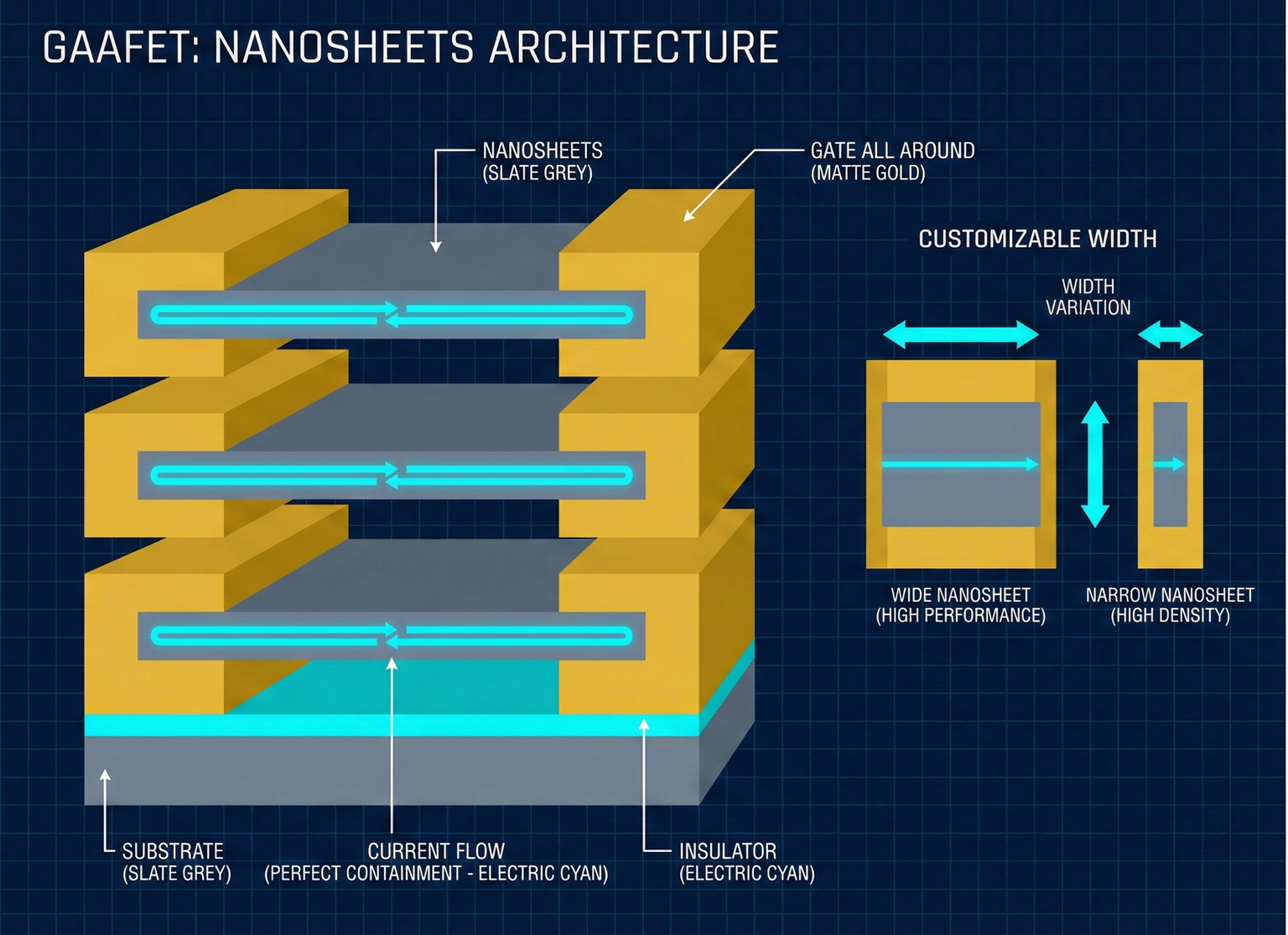
The Hidden Magic of Nanosheets: Designers' Favorite
GAA not only solves leakage current issues, but it also brings a huge commercial benefit: the channel width is 'continuously adjustable'.
In the FinFET era, the size and width of the fins were fixed (limited by the foundry's process). If you (e.g., a designer at Apple or MediaTek) needed a slightly larger current, you could only add fins one at a time (going from 1 fin to 2 fins). What if you only needed '1.5 fins' worth of current? Sorry, you would be forced to use 2 fins. This is called Quantized Width, and it wastes valuable space and power.
However, under the GAA architecture, nanosheets are 'drawn' by lithography machines, and their width is entirely determined by the designer:
- Efficiency Core (E-Core): Draw narrower nanosheets for extreme power saving.
- Performance Core (P-Core): Draw wider nanosheets (like wide noodles) to provide powerful computing current.
This gives MediaTek and Apple unprecedented freedom when designing chips, allowing them to optimize PPA (Performance / Power / Area) to the extreme.
📊 Strategic Summary: The Battle for Control
Here's a table summarizing the three generations of transistor architecture evolution over the past half-century:
| Characteristic | Planar FET (Traditional) | FinFET (Fin Field-Effect) | GAA (Gate-All-Around) |
|---|---|---|---|
| Era | > 20 nm and older | 16 nm – 3 nm | Below 2 nm |
| Structure Shape | Flat-lying pipe | Vertically standing fin | Suspended lasagna (stacked) |
| Control Surfaces | 1 surface (top only) | 3 surfaces (top/left/right) | 4 surfaces (360-degree coverage) |
| Leakage Control | Collapsed | Excellent | Physical limit of perfection |
| Design Flexibility | High (continuous width) | Low (limited fin count) | Extremely High (Nanosheet width freely adjustable) |
| Manufacturing Difficulty | Normal | Difficult | Hellish (requires suspended etching) |
| Strategic Masterpiece | TSMC 28nm (Golden Cash Cow) | TSMC N3, Intel 7 | TSMC N2, Samsung 3GAE |
Ultimate Revelation: GAA is not an option; it is a physical necessity to sustain Moore's Law. Whoever can be the first to implement it while maintaining high yields will secure dominance in the semiconductor industry for the next decade.
Samsung eagerly rushed to adopt GAA at 3 nm, attempting a curve overtake, but ended up crashing due to excessive manufacturing difficulty, with abysmal yields; whereas TSMC chose a conservative approach, pushing FinFET's potential to its extreme (extending its use through 3 nm), and only officially transitioning to GAA at 2 nm.
In-depth Research · Quantitative Perspective
Want more quantitative research insights on semiconductors?
[Insight Subscription Plan] Bid Farewell to Retail Investor Mindset: Build Your Alpha Trading System with "Quantitative Chips" and "Consensus Data"EDGE Semiconductor Research
📍 Series Map — Navigate the Complete EDGE Semiconductor Research →


