Preamble: Micro-architecture Defying Gravity
In the previous chapter, we arrived at a physical conclusion: to completely eliminate the ghost of leakage current, we must suspend the channels and have the gate fully encompass them 360 degrees without blind spots. This is the ultimate form of GAA (Gate-All-Around).
However, for engineers, drawing the blueprint is simple; the real challenge is "How do we actually build it?"
You cannot simply conjure a suspended channel out of thin air. On a flat silicon wafer, you need to construct nano-buildings with completely suspended floors, devoid of any pillar support.
This sounds like a challenge to gravity, but semiconductor engineers' solution is remarkably ingenious: first addition, then subtraction, and finally addition again.
We will leverage the minute chemical property differences between two materials (silicon and silicon-germanium) to play a "nanoscale Jenga game" in the cleanroom, a process costing hundreds of billions of New Taiwan Dollars.
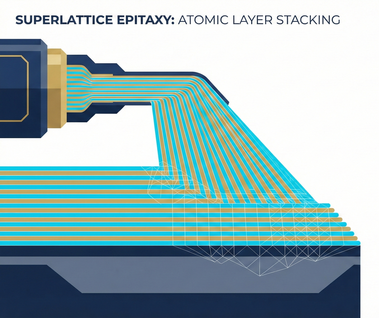
Step One: Superlattice Epitaxy — Baking a Nanoscale Layer Cake
- Task: Create the initial 3D scaffold.
- Core Equipment: Epi Reactor.
- Dominant Players: Applied Materials, ASM International (ASMI).
To create suspended structures on the wafer, we must first grow a "layer cake". Engineers select two materials with extremely similar lattice sizes, yet possessing critical chemical differences:
- Material A: Pure Silicon (Si) → The "channel" to be retained in the future.
- Material B: Silicon-Germanium (SiGe) → The "sacrificial layer" destined to be dissolved in the future.
Process Logic:
On the silicon substrate, the equipment precisely deposits a layer of SiGe, followed by a layer of Si, then another layer of SiGe, and another layer of Si... repeating this alternating stack 3 to 4 times.
Simple Analogy for Investors: The Scaffolding Philosophy of a Sandwich
Imagine you are making a premium sandwich. Pure silicon (Si) is the expensive, top-grade Wagyu beef you want to eat. Silicon-germanium (SiGe) is just the cheap toast bread.
To stack the Wagyu beef layer by layer without collapsing, you must first sandwich them with toast, using it as "scaffolding" for support.
Technical Challenge:
This is not merely ordinary coating. The thickness of each layer must be controlled to single-digit nanometers, and the atomic arrangement (lattice) of silicon and silicon-germanium must be "perfectly aligned (Epitaxy)." If even a single atom is misplaced, the future electrical current will encounter a collision there.
This has led to explosive growth in demand for epitaxy equipment in the 2-nanometer generation.
Step Two: Fin Patterning — Cutting the Layered Walls
- Task: Carve out the preliminary shape of the building.
- Core Equipment: Plasma Dry Etcher.
- Dominant Player: Lam Research.
Now we have a perfectly flat layer cake; the next step is to cut it into long, strip-like walls.
Process Logic:
Apply photoresist, call upon ASML's EUV lithography machine to draw extremely fine line blueprints, and then let Lam Research's plasma etcher, like an invisible nanoscale samurai sword, mercilessly cleave downwards vertically, cutting out deep trenches.
At this stage, rows of "layered walls" stand upright on the wafer. Please note that at this point, the pure silicon (Si) and silicon-germanium (SiGe) are still tightly bonded together, forming a solid body.
Step Three: Inner Spacer — The Insulating Rubber Ring Against Leakage
This step is often omitted in most popular science articles, but it is actually critical for the survival of GAA chips and is extremely difficult, essentially a "micrometer-scale caulking engineering" task.
Before we completely remove the scaffolding (SiGe), we must protect the future Source/Drain regions.
Because the future metal gate and the conductive Source/Drain are too close, if they are not separated, a short circuit and burnout could occur the moment power is applied.
Process Logic:
Engineers will first slightly etch the SiGe inwards from the side of the layered walls, creating a tiny recess. Then, into this minuscule groove, they precisely fill a layer of low-k dielectric insulating material.
Simple Analogy for Investors: The Faucet Rubber Gasket
Imagine the interface between a metal faucet handle and the water pipe. Without that black rubber gasket, no matter how tightly the faucet is screwed, water would still seep out from the gaps.
The Inner Spacer is the most precise rubber gasket in the GAA structure, responsible for tightly insulating the future switch from the channels.
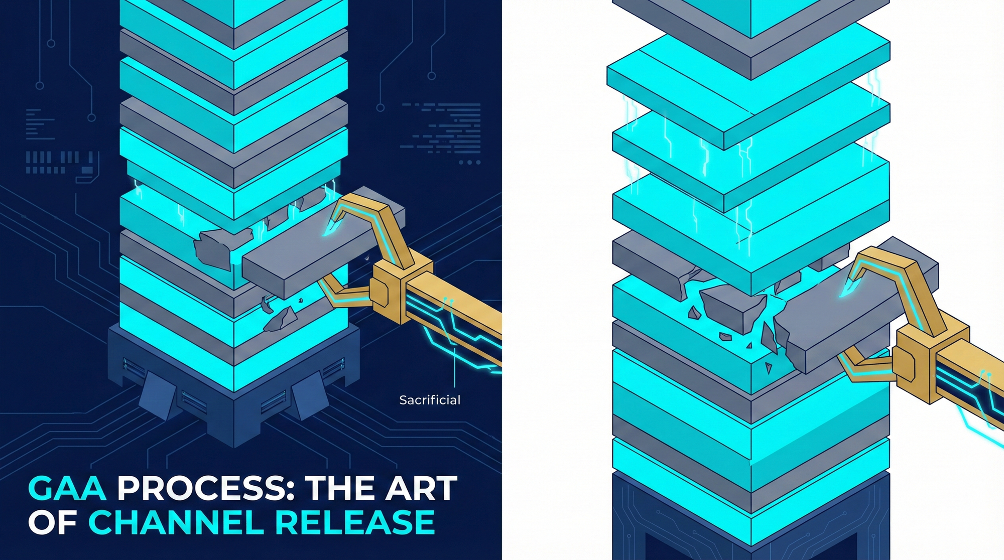
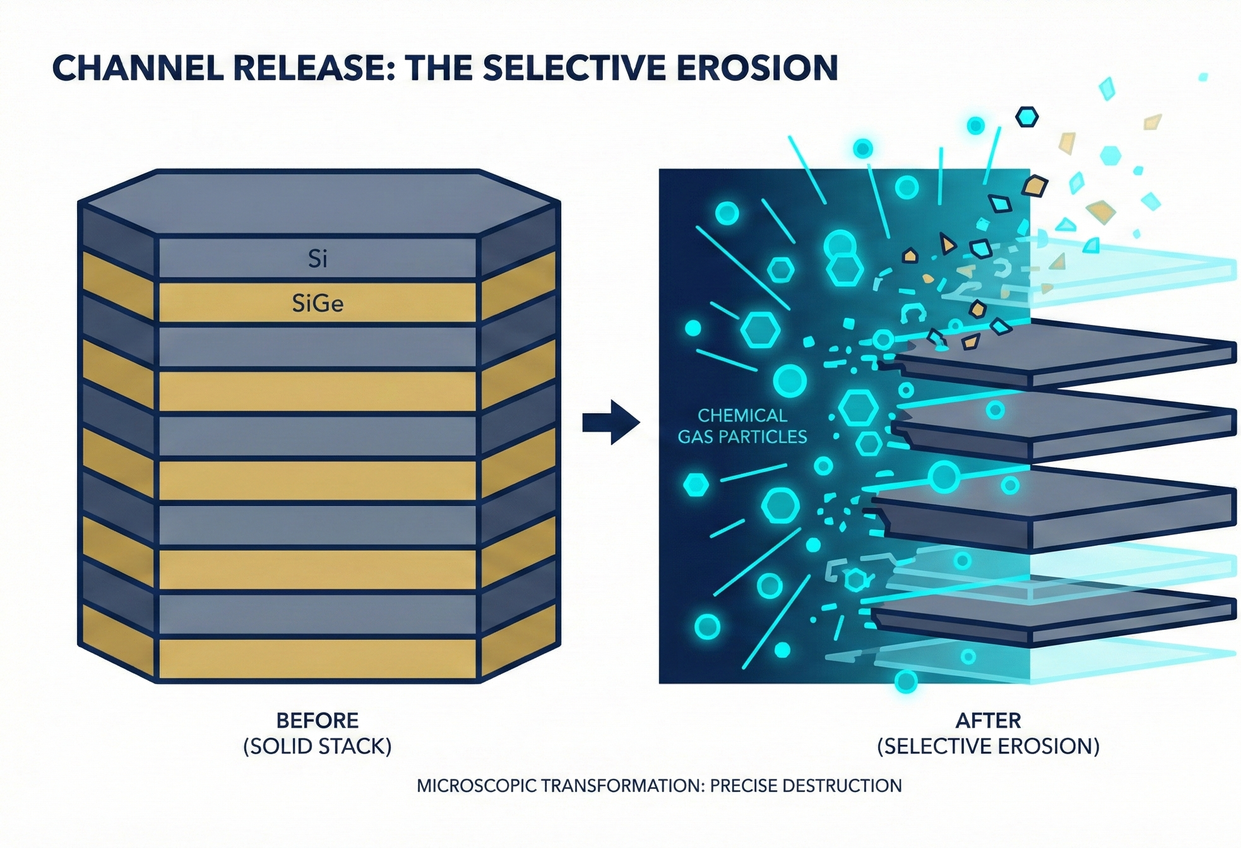
Step Four: Channel Release — The Ultimate Jenga Magic
- Task: Make the nanosheets truly suspended.
- Core Equipment: Selective Etcher.
- Dominant Player: Lam Research (proprietary technology).
This is the true "gate of hell" for TSMC's 2nm and Samsung's 3nm processes. We are about to perform the magic of transforming a solid building into suspended floors.
Challenge:
We need to dissolve all the SiGe (scaffolding) sandwiched in between, but we must absolutely not damage the pure silicon (Wagyu beef channels) layers above and below. Even if 0.1 nanometer of pure silicon is etched away, the chip's performance could be completely ruined.
Technical Solution: High Selectivity Isotropic Etch
Lam Research has developed a special chemical gas formula for this purpose. This gas is severely "picky": it has an insatiable appetite for Germanium (Ge) but almost no interest in pure Silicon (Si).
When the wafer is exposed to this gas, the gas acts like swarms of nanoscale termites, drilling into the sides of the layered walls and devouring only the SiGe layers (hollowing them out).
Simple Analogy for Investors: Nanoscale Jenga
You are playing a game of Jenga on an invisibly small scale. You need to instantaneously remove all the middle blocks (SiGe), but the blocks above (Si) must not only remain standing but also show no scratches on their surface.
When the gas dissipates, the original pure silicon layers are miraculously suspended in mid-air, becoming perfect nanosheets.
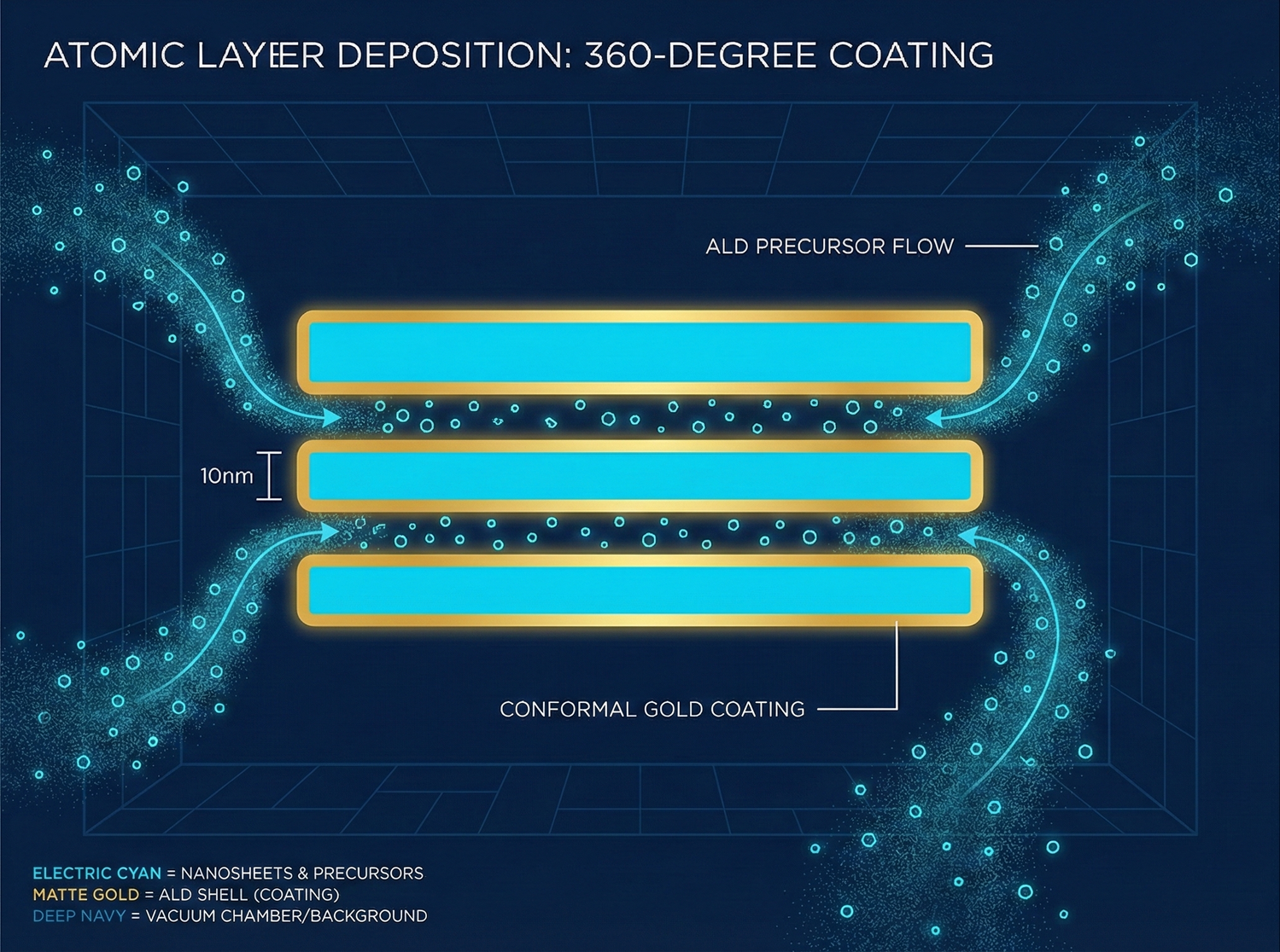
Step Five: HKMG Deposition — Atomic-Level Extreme Painting
- Task: Install the fully wrapped gate (valve).
- Core Equipment: ALD (Atomic Layer Deposition equipment).
- Dominant Players: ASM International (ASMI.AS), Tokyo Electron (TEL).
Now that the nanosheets are suspended, the final step is to insert the metal gate, encompassing each suspended nanosheet 360 degrees without blind spots.
Critical Pain Point: Crevice Phobia
The gaps between these suspended nanosheets can be as narrow as 10 nanometers.
- Using traditional PVD (Physical Vapor Deposition, like spray painting) would cause metal atoms to get stuck at the opening, sealing off the gap.
- Using traditional CVD (Chemical Vapor Deposition), the film growth rate is too fast, easily leading to uneven thickness.
Solution: ALD (Atomic Layer Deposition) steps in
We can only rely on the slowest, yet most precise, ALD technology. This technique uses special gas molecules to deposit atoms layer by layer, slowly building up the film.
First, a High-k insulating layer (such as hafnium oxide) is grown, followed by a layer of metal gate (such as tungsten or titanium alloy).
Simple Analogy for Investors: Painting the Underside of a Suspended Bridge in a Hurricane
You are asked to paint a suspended bridge, and you must paint the entire underside and crevices of the bridge, with the thickness limited to exactly one atom's worth.
ALD gas, like an invisible ghost, slowly penetrates the extremely small gaps of the nanosheets, evenly coating every surface (top, bottom, left, right) with atoms.
2-6-2 Strategic Summary: The Armaments Dealer Power Map for GAA
Understanding this building craftsmanship reveals why TSMC's 2-nanometer fab capital expenditure may reach a historic high, and which equipment suppliers are poised for structural explosive growth.
| Step | Core Process | Physical Challenge | Absolute Dominant Player (Ticker) | Wall Street Investment Logic |
|---|---|---|---|---|
| 1. Epitaxy | Superlattice | Precise control of Si/SiGe atomic-level thickness | Applied Materials, ASMI | Epitaxy steps double in the GAA era, directly boosting equipment demand. |
| 2. Patterning | Fin Etch | Vertical deep trench etching | Lam Research, TEL | Continuation of traditional strengths, steady capital expenditure benefits. |
| 3. Release | Selective Etch | Etches only the scaffolding, not the channels (high selectivity) | Lam Research (LRCX) | 🔥 Strongest Moat. Without Lam's proprietary gas, GAA suspended structures cannot be made. |
| 4. Deposition | ALD (HKMG) | Filling extremely narrow nanoscale suspended gaps | ASMI (ASMI.AS) | 🔥 Growth Explosion King. GAA structures are too complex, making ALD the only solution for gap filling. ASMI virtually monopolizes this market. |
Ultimate Insight: The Deadly Squeeze of the Process Window
GAA manufacturing is a tightrope walk where no mistakes are permitted.
If the SiGe is not completely removed during channel release (residue), or if even a tiny bubble (void) is left during ALD gap filling, this AI chip, valued at hundreds of dollars, could be immediately scrapped.
This is why GAA's yield rate is extremely difficult to improve.
This also raises an age-old dilemma: as a foundry, should one venture into GAA early, or hold onto FinFET until the last moment?
In-Depth Research · Quantitative Perspective
Want more insights into semiconductor quantitative research?
【Insight Subscription Plan】Break Free from Retail Investor Mentality: Build Your Alpha Trading System with "Quantitative Chips" and "Consensus Data"EDGE Semiconductor Research
📍 Series Map — Navigate the Complete EDGE Semiconductor Research →


