Transition: From the Cleanroom Back to the Business Negotiation Table
After understanding the magical "suspended building construction" of GAA, we can finally shift our focus from the cleanroom back to the brutal business negotiation table.
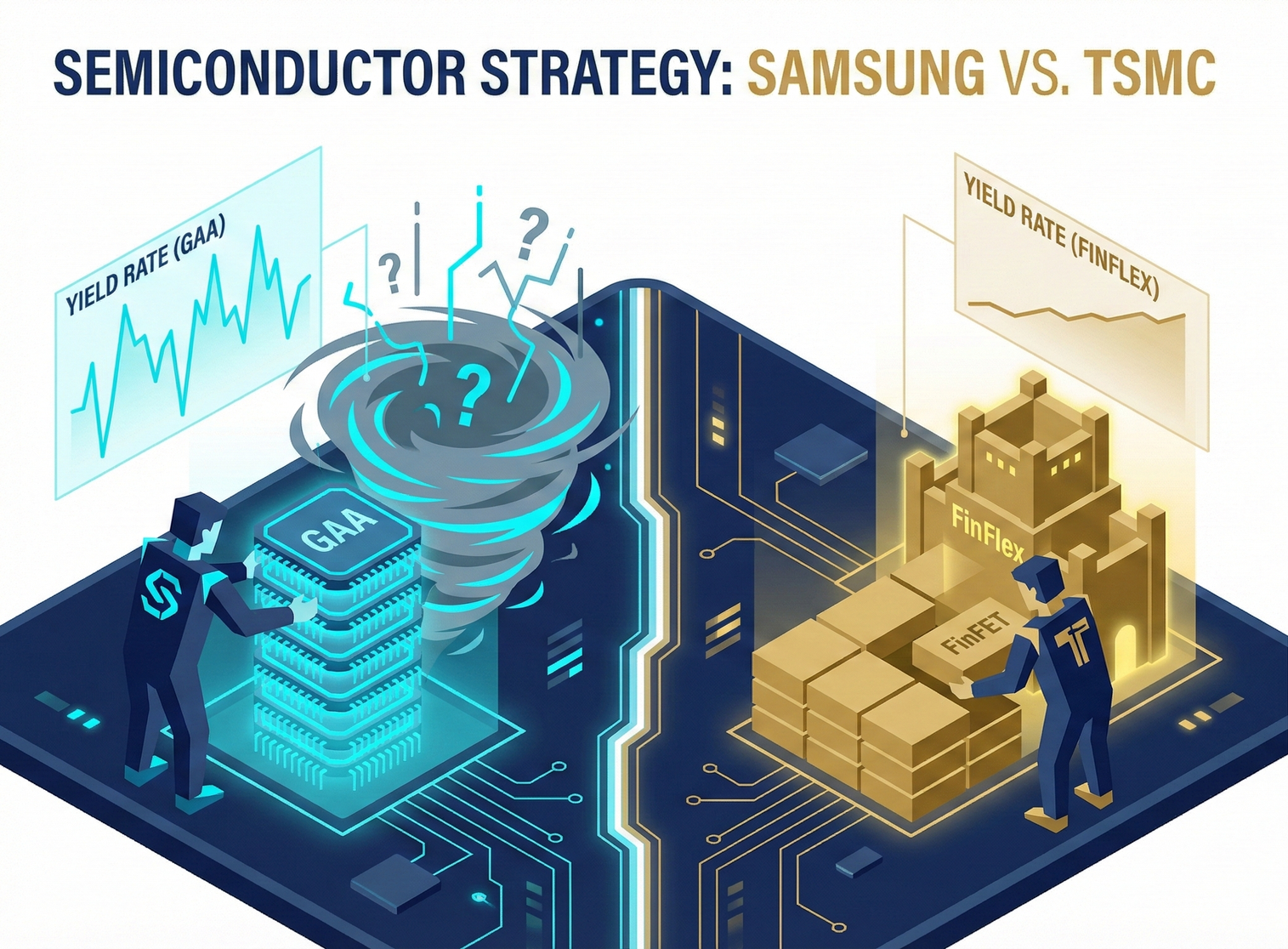
There is an extremely dangerous misconception in the semiconductor industry: whoever adopts new technology first is the winner.
This statement was regarded as a golden rule by Samsung in 2022, but it was brutally disproven by TSMC's stark financial reports in 2024.
In 2022, Samsung held a high-profile global press conference, announcing the first mass production of its 3nm GAA architecture (code-named 3GAE) and proudly claimed to be "a full six months ahead of TSMC" in transistor architecture.
However, by 2024, the harsh reality was that TSMC's seemingly "conservative" 3nm (FinFET architecture) capacity was snapped up by Apple, NVIDIA, and Qualcomm with cash in hand; while Samsung's 3nm GAA fabs were largely idle, with yields languishing at low levels, and even its own mobile division dared not fully commit its flagship chips to it.
Why? Because Samsung committed a cardinal sin in semiconductor strategy: forcibly pushing a new architecture at the physical limit onto an immature ecosystem.
Chapter One: Samsung's Waterloo
Samsung's strategic logic was actually quite dramatic: overtaking on the curve.
Samsung's executives clearly understood that during the FinFET era (from 14nm to 5nm), they had been completely surpassed by TSMC in yield and power consumption control.
If they continued to follow TSMC with FinFET for 3nm, they would forever be stuck with TSMC's leftover orders (always being the perennial second-place). Therefore, Samsung decided to go all-in, skipping 3nm FinFET and betting everything on GAA.
But the laws of physics are unforgiving. This high-stakes gamble ultimately turned into a disaster.
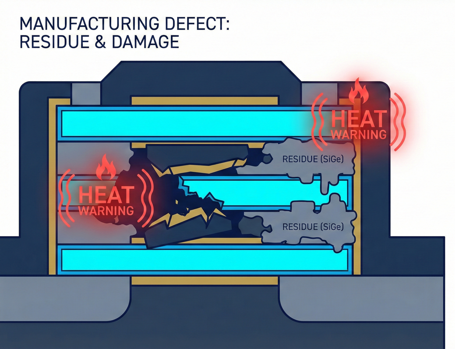
1) The Physical Truth Behind Yield Collapse: The Failure of "Jenga"
Do you recall the "channel release (Jenga)" we discussed in 2-6-2? It involves perfectly dissolving away the silicon-germanium (SiGe) to leave suspended pure silicon (Si) nanosheets.
Samsung's fatal flaw occurred at the critical juncture of this "selective etching" process.
- Variability Curse: Samsung's etching gas formula and equipment control had issues. Sometimes the SiGe wasn't completely dissolved, leaving residues in the gaps. Other times, the etching was too aggressive, eroding parts of the silicon nanosheets that were meant to be preserved.
- Fatal Consequence: This resulted in hundreds of billions of "taps" on the chip, each with a different "aperture." Some leaked, others were blocked.
For smartphone chips (SoCs) that demand absolute consistency and are highly sensitive to leakage, this meant the chips would inexplicably overheat and crash.
This sent shivers down Qualcomm's spine, and they promptly transferred their orders back to TSMC overnight.
2) Ecosystem Breakdown: An Isolated Advance Without Logistics
TSMC often states, "We do not compete with our customers," but Samsung not only competes with its customers (having its own Exynos chips and Galaxy phones), it even neglected the preparation of the software ecosystem.
- When Samsung aggressively pushed GAA, the world's two largest EDA (Electronic Design Automation) software giants, Synopsys and Cadence, had not yet fully optimized their simulation tools for GAA.
- Design House Fear: Engineers at Apple or NVIDIA found that to use Samsung's 3nm GAA, they would have to "completely redraw" circuit diagrams worth billions in R&D costs, and the software could not guarantee reliable results.
In contrast, continuing with TSMC's FinFET, old designs only required minor modifications to go straight into production. Who would risk being Samsung's guinea pig?
3) False 'Mass Production'
Samsung's claimed "world's first mass production" was actually more of a PR stunt. Initial customers were Chinese Bitcoin mining chips.
The strategic interpretation is ruthless: The structure of mining chips is extremely simple and repetitive; if a few blocks are faulty, they can be directly shielded, and the chips can still be sold with reduced computing power. Samsung was effectively using low-end customer wafers for "training" and "debugging."
It's no wonder that even Samsung's own flagship smartphones to this day still have to dutifully purchase TSMC-manufactured Snapdragon chips from Qualcomm.
Chapter Two: TSMC's Calculation
Roadmap Code: N3 (Ultimate FinFET) → N2 (Official GAA)
TSMC's decision-making logic is cold and precise: customers pay for tangible improvements in PPA (Performance/Power/Area), not to hear your sci-fi stories about GAA.
If FinFET could still be squeezed for every last drop of value, why should customers bear the enormous risks of transitioning to a new architecture?
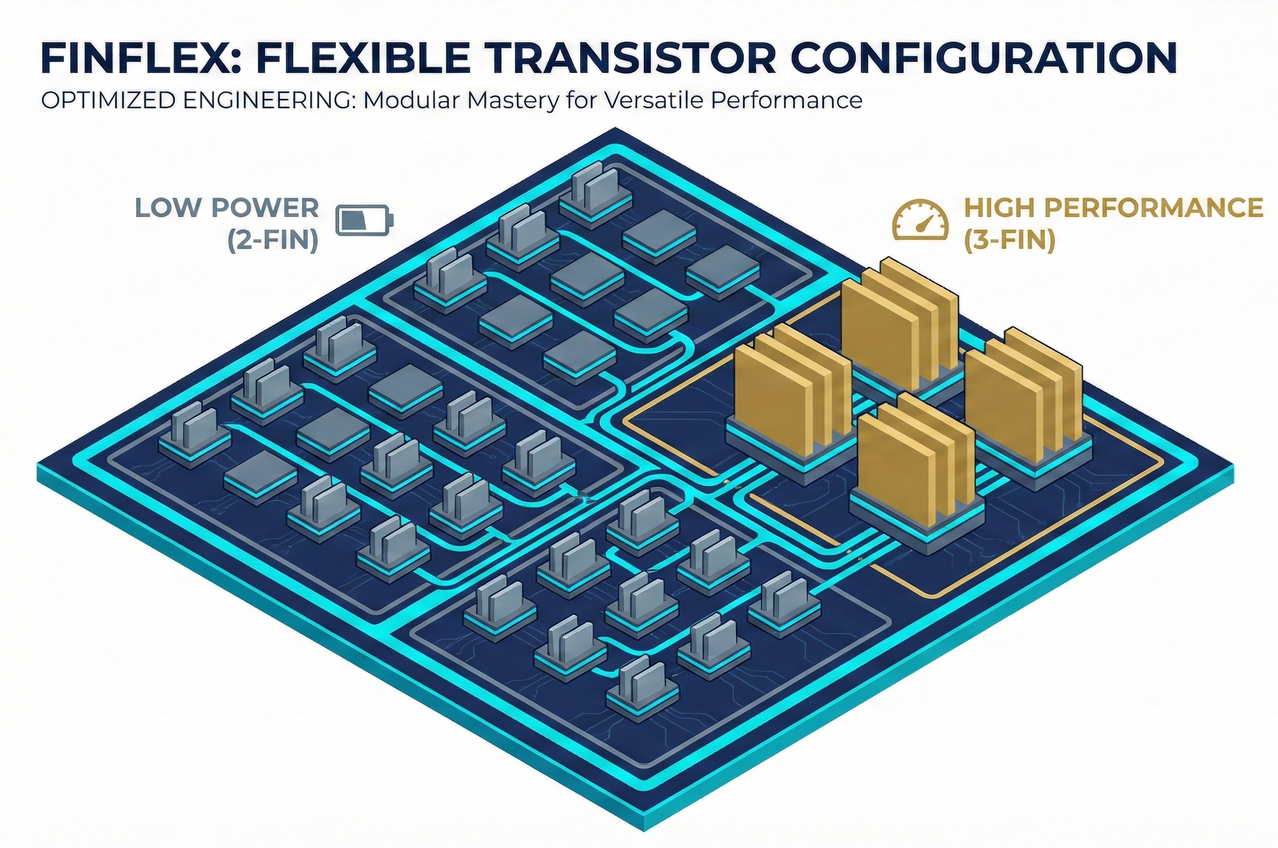
1) The N3 Miracle: FinFlex (Flexible Fin Combination)
While TSMC continued to use FinFET for 3nm, it wasn't sitting idly by, but instead invented FinFlex.
- Technical Details: In previous FinFET designs, only one fin configuration could typically be chosen for a given area (e.g., all 3 fins for high performance but high power consumption).
- Layman's Analogy: Customized LEGO mixing and matching. TSMC broke this limitation, allowing designers to freely mix standard cells of "2-1 Fin (extremely power-efficient)" and "3-2 Fin (extreme performance)" within the same chip, or even within the same logic block.
This means Apple can use smaller "LEGO bricks" for the power-saving cores on a chip, and larger "LEGO bricks" for the performance cores.
- Strategic Outcome: Thanks to this architectural modification, TSMC's N3 actually delivered performance and power consumption results that could outperform Samsung's 3nm GAA, with initial yields exceeding 80%.
TSMC used the most stable existing technology to capture the fattest profits in the market.
2) N2's Advance: NanoFlex Debuts
By the end of 2025, TSMC is set to officially introduce GAA for its 2nm (N2) process.
Why now? Because by this time, equipment from Applied Materials and Lam Research has been "tested" and matured by Samsung, and Synopsys's software is also ready.
TSMC waited for the ecosystem to roll out the red carpet before making its entrance with ease.
- Technology Upgrade: NanoFlex. This is the GAA version of FinFlex.
TSMC allows chip designers in the N2 process to freely adjust the "width of the nanosheets" (short channels for extreme power efficiency, wide channels for ultimate speed). This technology will become the absolute main force for Apple's iPhone 17 processors and NVIDIA's next-generation Rubin AI chips.
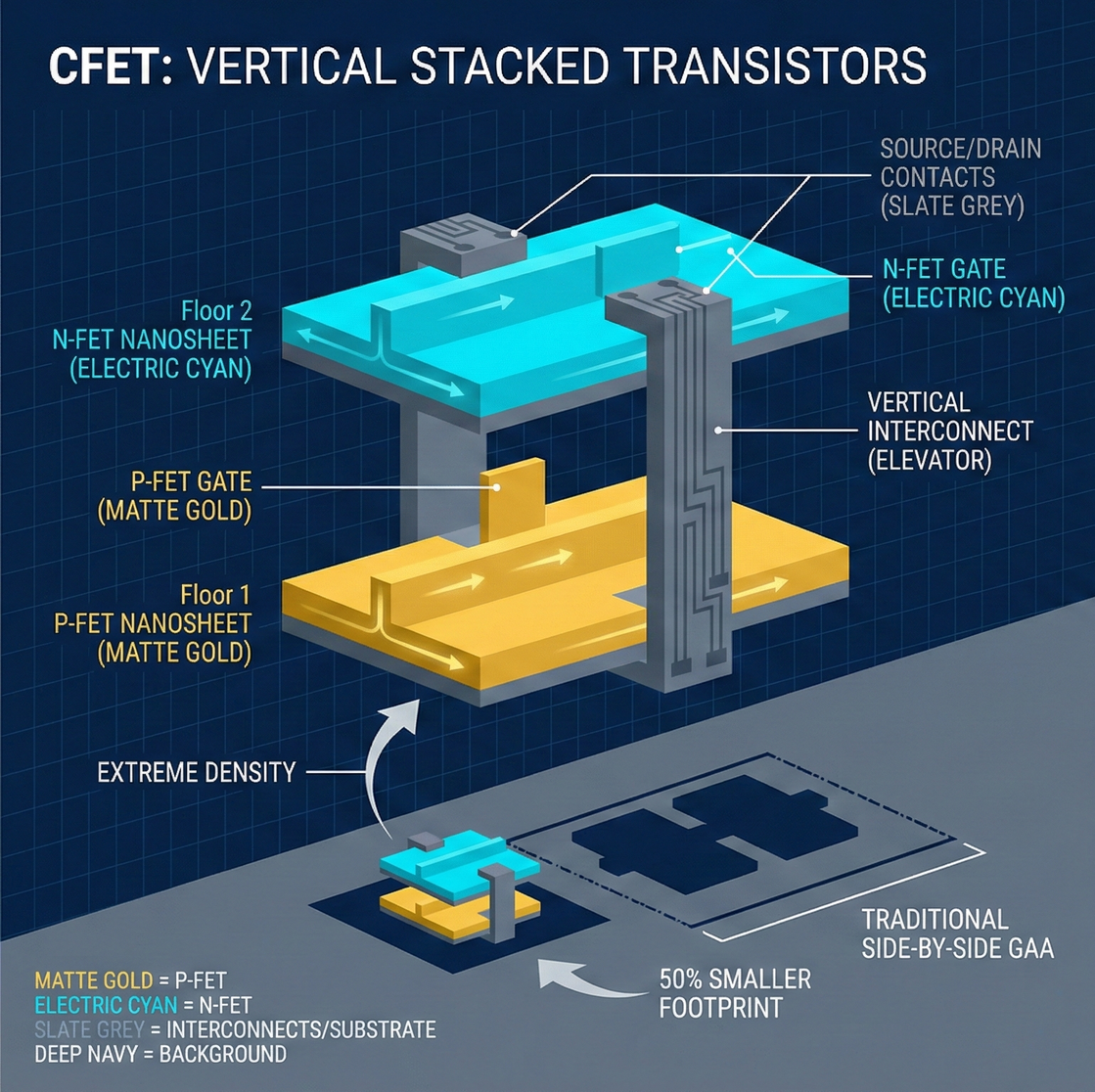
Chapter Three: Endgame Battle — CFET (Complementary Field-Effect Transistor)
Generation Code: A10 (1nm or Angstrom Generation)
While GAA is the savior for 2nm, the grim reaper of physical limits never stops approaching.
GAA solved the leakage problem (the "taps" are tightly closed), but it still "unfolds flat" on the wafer surface. An N-type transistor and a P-type transistor still have to lie side-by-side on the silicon wafer, occupying "two parking spots."
By the 1nm (A10) generation, even GAA will no longer be sufficient.
To continue miniaturization, humanity must develop along the Z-axis (upwards).
1) Structural Revolution: Stacking Houses
- CFET (Complementary FET): vertically stacks N-type and P-type transistors.
- Layman's Analogy: Double-decker bus and bunk beds.
- GAA: Two single beds placed side-by-side in a room (occupying double the area).
- CFET: Changes to bunk beds. P-FET on the first floor, N-FET on the second floor. Logic area instantly slashed by 50%.
- Hell-Level Physical Difficulty: After building the first-floor nanosheets, you must precisely build the second-floor nanosheets directly above, and vertically connect the metal lines between the first and second floors.
This requires an overlay accuracy for KLA inspection machines that will approach "atomic levels."
2) Who is Planning for Future Double-Decker Buses?
- imec (Interuniversity Microelectronics Centre, Belgium): Has demonstrated initial CFET prototypes.
- Intel: Having lagged behind in both FinFET and GAA generations, is investing extremely aggressively, with CFET seen as the ultimate weapon for a comeback after 2030.
- TSMC: Remains calm and steady, expected to extract every last drop of value from GAA, only passing the baton to CFET at the A14 or A10 (1nm) node, or even later.
2-6-3 Strategic Summary: Structure is Destiny
This table encapsulates the chip war of the next 5 years. What determines victory is no longer who issues the first press release, but who can translate physical limits into commercial profit.
| Node | Technology Architecture | Samsung | TSMC | Battle Assessment & Commercial Reality |
|---|---|---|---|---|
| 3nm | FinFET vs. GAA | 3GAE (GAA): Low yields, no major international clients dared to tape out. | N3 (FinFET): With FinFlex, extremely high yields, capturing Apple/NVIDIA/Qualcomm orders. | TSMC complete victory. Proved that the commercial value of "maxing out old technology" far outweighs "immature new technology." |
| 2nm | GAA (Nanosheet) | SF2: Attempting to correct 3nm errors, aiming to win back old customers. | N2: Official introduction of GAA combined with NanoFlex, full ecosystem support. | Decisive point. TSMC is expected to maintain its dominance with its vast IP library and high-yield ecosystem. |
| 1.4nm | Continuation of GAA structure | Follower, facing capital expenditure pressure. | A14: Ultimate GAA version, beginning evaluation of High-NA EUV equipment. | Intel will attempt a fierce counterattack at this node (14A) with new equipment. |
| 1nm | CFET (Vertical Stacking) | Under development. | A10: Bunk-bed structure, breaking through 2D area limits. | Entering the Angstrom Era, physical manufacturing difficulty reaches its peak. |
Implications for Investors
- The Pioneer's Curse: Samsung's disastrous 3nm GAA case proves that in the semiconductor industry, "being quick is not as good as being stable." Venturing into a physical forbidden zone without software and equipment support will only turn hundreds of billions in capital expenditure into ashes of yield collapse.
- The Ecosystem is the True Moat: TSMC wins not just on manufacturing technology; it wins through a grand alliance called OIP (Open Innovation Platform).
- ASML helps it fine-tune equipment.
- Synopsys helps it write software.
- ARM helps it design IP.
Clients just need to hand over their blueprints to TSMC, and the rest is waiting to collect revenue. This moat, woven from trust and mutual benefit, remains difficult for Samsung and Intel to cross.
In-depth Research · Quantitative Perspective
Want to gain more insights into semiconductor quantitative research?
【Insight Subscription Plan】Bid Farewell to Retail Investor Mentality: Build Your Alpha Trading System with "Quantitative Chips" and "Consensus Data"EDGE Semiconductor Research
📍 Series Map — Navigate the Complete EDGE Semiconductor Research →


