In the previous chapter of the 2-6 series, we pushed humanity's physical limits, finally elevating transistors from 2D planar structures to 3D FinFETs, and ultimately even hollowing out the foundation to create GAA (Gate-All-Around) structures suspended in mid-air.
We succeeded. We created the universe's most perfect "nanoscale faucet," completely eliminating the specter of quantum leakage.
But now, looking at this perfect blueprint, top architects at wafer fabs face an extremely awkward and decades-old critical crisis that no one has dared to touch: "No matter how exquisitely rooms are built, if the building's elevators are jammed or the electrical wiring catches fire, the building is still useless."
This is the semiconductor industry's unspoken secret: the miniaturization of transistors accounts for only half of Moore's Law; the other half of the nightmare is called "routing."
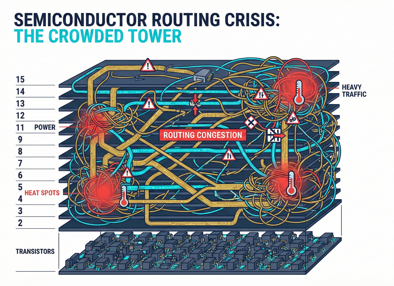
1. The True Structure of a Chip Building: The Crowded Rooftop
To understand this crisis, we must first comprehend the true three-dimensional structure of a chip. Chip manufacturing is divided into two major stages:
- Front-End-of-Line (FEOL): This is the process of building transistors (faucets) on the "ground floor" of the silicon wafer.
- Back-End-of-Line (BEOL): After completing the ground floor, engineers must build a network of over a dozen layers of metal interconnects "above" the transistors.
You can imagine a chip as a 15-story high-rise office building. The first floor houses the employees responsible for computation (transistors), while floors 2 to 15 are entirely filled with densely packed corridors, elevators, and pipelines.
Within this pipeline system, two entirely different things flow:
- Signal: This is the information employees use to communicate with each other (0s and 1s for logical operations).
- Power: This is the employees' lunchbox (Vdd power supply and Vss ground).
For over sixty years, the semiconductor industry has had only one rule: whether it's information or lunchboxes, everything must be delivered downwards from the building's "rooftop (top layer)."
2. Physical Collapse: When Signals and Power Clash in the Corridors
Before 7 nanometers, this rule worked well. But as process technology advanced to 3 nanometers, and even 2 nanometers (N2), disaster struck.
The transistors on the first floor became too small and too dense. Billions of employees crammed onto the first floor, requiring enormous amounts of power (lunchboxes) while also frantically exchanging signals (information). As a result, the elevators and corridors upstairs became completely congested. Worse still, the "thick wires" responsible for power delivery and the "thin wires" responsible for signal transmission became intertwined, leading to two fatal physical effects:
- Routing Congestion: Designers discovered that the chip's area could no longer be shrunk. Not because the transistors on the first floor couldn't be miniaturized, but because "the wires upstairs couldn't be arranged"! The power delivery network (PDN) surprisingly occupied as much as 20% to 30% of the routing space. This is like a building where, to accommodate cargo elevators for delivering lunchboxes, employees are forced to sacrifice even their desks.
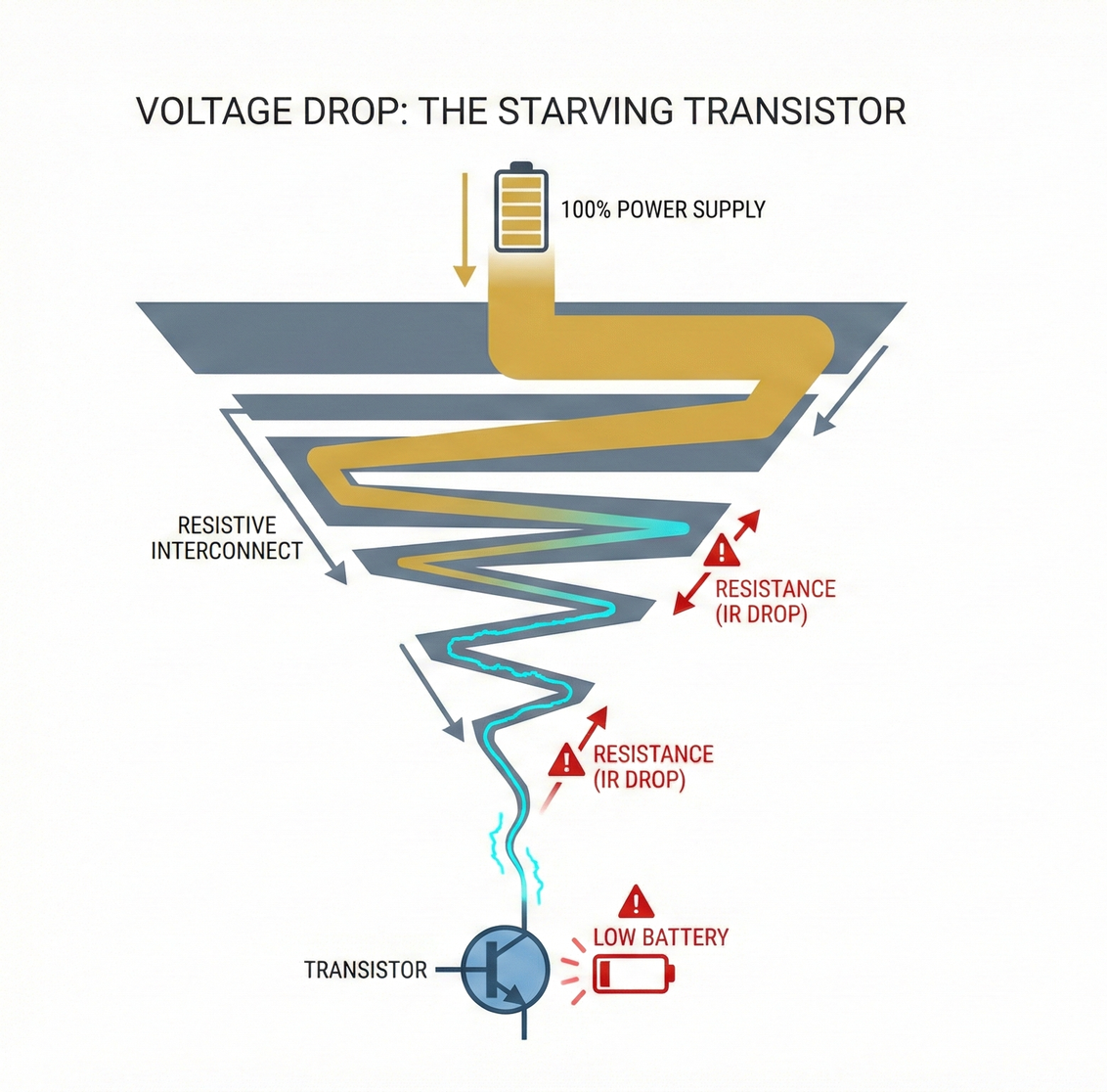
- IR Drop: This is the most critical physical curse. When metal wires become only a few nanometers thick, resistance rapidly skyrockets. As high voltage is transmitted all the way down from the 15th-floor rooftop, passing through layers of wires thinner than hair, by the time it finally reaches the transistors on the first floor, the voltage has been largely consumed by the resistance along the path (converted into waste heat). Result: Transistors are unable to operate at full speed due to "undernourishment (insufficient voltage)," and may even produce computational errors.
3. The Great Escape of Thought: The Radical Facelift of Flipping the Wafer
No matter how powerful the GAA faucet on the first floor is, if it can't deliver water, it's just a decoration. When architects at TSMC and Intel were pushed into a corner by this problem, they suddenly turned their attention to the "silicon wafer substrate" that supported everything.
Humanity has used silicon wafers for sixty years, but throughout these sixty years, we have only utilized the "thin top 1% layer" of the wafer to build our structures. The remaining 99% thickness of silicon purely served as a "foundation stone" for physical support, essentially useless.
A wild, audacious idea, akin to dissecting a semiconductor, was born: "Since the elevators upstairs are jammed, why don't we flip the entire building over, drill holes directly from the 'basement (backside of the wafer),' and deliver power to the first floor?"
This is the nuclear weapon that will completely rewrite the trajectory of Moore's Law from 2025 to 2026—the Backside Power Delivery Network (BSPDN).
Let information (signals) continue to use the rooftop, and let lunchboxes (power) use the underground pathway. Signals and power are completely separated, without interference.
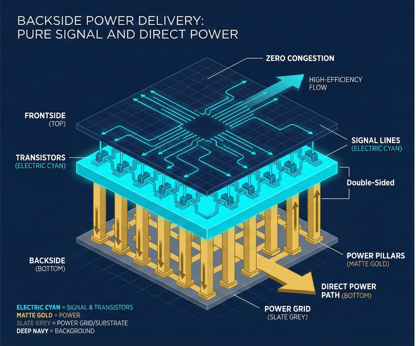
This sounds incredibly elegant, but in a cleanroom, it means engineers must flip the wafer, ruthlessly grind away that 99% useless silicon substrate layer, then precisely drill nanoscale deep holes into the "backsides" of billions of transistors, and finally inject liquid metal into them.
This is an extreme backside wafer facelift. Next, we will unveil the "Backside Power Delivery War" led by TSMC's A16 process and Intel's 18A process. In this battle, Intel aims to overtake its rivals with it, while TSMC has prepared even more formidable countermeasures.
In-Depth Research · Quantitative Perspective
Want more insights into semiconductor quantitative research?
【Insight Subscription Plan】Break Free from Retail Investor Thinking: Build Your Alpha Trading System with "Quantitative Chips" and "Consensus Data"EDGE Semiconductor Research
📍 Series Map — Navigate the Complete EDGE Semiconductor Research →


