In the semiconductor industry's 60-year history, regardless of how Moore's Law evolved, whether from Planar to FinFET or GAA, the world's top engineers have quietly adhered to an unquestioned iron rule: "Frontside Power Delivery."
This iron rule means that all of a chip's "organs" (transistors responsible for computation) are built on the bottom layer of the silicon wafer; while all "blood vessels" (metal interconnects) responsible for delivering nutrients are layered one by one on top of the transistors.
This is like a highly developed microscopic city. Whether it's signal wires transmitting confidential data or power wires delivering massive amounts of electricity, all are crammed into the frontside metal layers of the chip, sharing the same set of corridors and elevators.
Before 7nm, everyone coexisted peacefully. But as manufacturing processes advanced to 3nm and 2nm, this skyscraper became too tall and its population too dense. This 60-year-old iron rule finally encountered a complete collapse due to physics and geometry.
🏙️ Chapter One: The Maze of BEOL — The Turf War Between Signals and Power
In wafer manufacturing, the step of building the bottom layer of transistors is called FEOL (Front-End-of-Line); the subsequent massive engineering task of "drawing metal lines" is called BEOL (Back-End-of-Line).
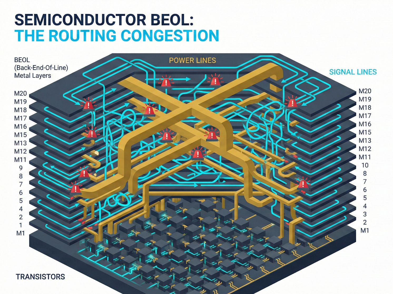
1. The True Structure of a Nanometer Skyscraper
If we dissect an advanced AI chip, it's an extreme skyscraper with 1 basement level and 15 to 20 above-ground floors:
- 1st Floor (FEOL): Home to tens of billions of residents (transistors). They are the only ones truly "working (computing 0s and 1s)" in this building.
- 2nd to 20th Floors (BEOL): These are densely packed corridors, stairwells, and elevators (metal interconnects made of copper or cobalt, M1 to M15+).
- Rooftop (C4 Bump): This is the sole entry point for external supplies (power and signals from the motherboard) into the building.
2. Congestion Crisis (Routing Congestion)
In the corridors of this building, two completely different types of pipelines run, and they have begun to fight for extremely scarce space:
- Signal wires need to be "numerous": As the number of transistors on the first floor explodes, they need extensive communication with each other. Signal wires are like countless couriers carrying confidential letters; they don't need wide paths, but they require extremely dense and intricate channels to crisscross between various floors.
- Power wires need to be "thick": Because advanced chips have enormous computational loads, they consume a lot of power (e.g., NVIDIA chips often draw hundreds of watts). Power wires are like massive high-pressure water pipes; if the pipes are too thin, not only is power delivery too slow, but they can also burn out due to high temperatures (Electromigration effect). Therefore, power wires must be very thick.
Current Collapse:
In the 2nm process, floor space (metal layer density) has been compressed to atomic limits. The tragedy occurred: those thick water pipes (power wires) ruthlessly occupied as much as 20% to 30% of the BEOL corridor space!
Consequences: The couriers (signals) have no path! Chip designers (such as MediaTek and Apple) were dismayed to find when drawing circuit diagrams that, to avoid the massive power lines, they were forced to make signal lines "take a longer route." This not only increased signal transmission delay, slowing down the chip, but also made it impossible to reduce the chip's total area further.
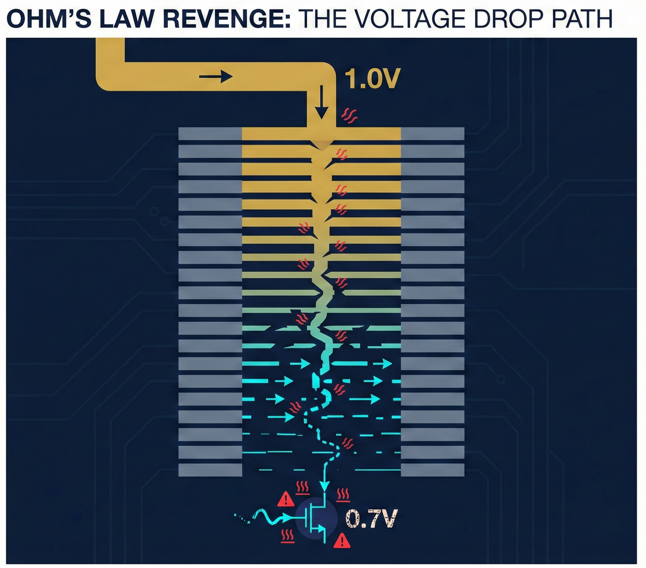
📉 Chapter Two: Ohm's Law's Revenge — IR Drop (Voltage Drop)
If spatial congestion merely gives designers a headache, then IR Drop (voltage drop) is directly fatal to the chip. This is classical physics' most relentless punishment for the limits of human miniaturization.
1. What is IR Drop?
According to the basic Ohm's Law formula:
$$V = I \times R$$
- $V$ (Voltage Drop): This refers to the voltage senselessly wasted or lost during transmission.
- $I$ (Current): Advanced chips require a very large total current to pursue ultimate computing power.
- $R$ (Resistance): This is the fatal flaw. The thinner the metal line and the longer the path, the exponentially higher the resistance.
2. The Long and Painful Journey of the Water Pipe
- Scenario: External power enters this 20-story building from the rooftop (C4 bump connection point), where the voltage is a full 1.0V.
- Path: This 1.0V voltage must drill downwards through M20 $\rightarrow$ M19 $\rightarrow$ M18... passing through over a dozen metal layers and tens of millions of extremely tiny metal contact points (Vias). Worse still, the closer it gets to the first floor, the thinner the metal lines become (to align with tiny transistors).
💡 Plain English Analogy for Investors: The Tragedy of the Daisy-Chained Water Hoses
Imagine your garden hose has extremely strong water pressure (1.0V). But to get the water to the farthest corner, you connect 20 hoses, and each hose is thinner than the last, finally snaking around the entire garden before reaching the spray gun.
The result is predictable: when you happily press the spray gun, the water flow is as weak as a dribble. All the water pressure was consumed by the friction (resistance) of the extremely thin hoses along the way.
Cruel Data and Consequences:
When the full 1.0V power, having endured this long, hellish journey, finally reaches the transistors on the 1st floor, the voltage may have dropped to 0.7V or even lower.
Transistors face a severe state of "undernourishment":
- Minorly, performance degradation: The transistors' switching strength is reduced, the Clock Speed cannot be increased, and chip performance is severely compromised.
- Severely, system crash: Excessively low voltage can lead to logic errors (a signal that should be 1 becomes 0), which would cause catastrophic system crashes in AI computing or autonomous driving. Simultaneously, all the lost voltage ($V$) is converted into waste heat, turning the chip into a high-temperature furnace.
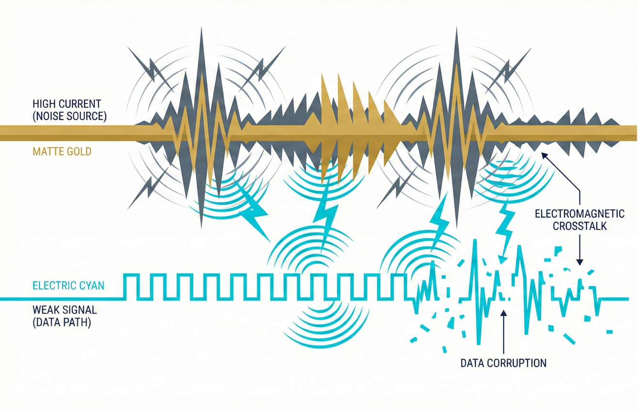
🔊 Chapter Three: Signal Interference — Noisy Neighbors
Beyond occupied space and voltage loss, bundling power lines and signal lines together also gives rise to a third invisible killer: noise interference.
1. The Nightmare of Electromagnetic Coupling
- Physical Phenomenon: When a conductor carries a rapidly changing large current, intense electromagnetic field fluctuations are generated around it.
- Scenario Comparison:
- Power Lines: Carry huge and extremely rapidly fluctuating currents (especially when a GPU instantaneously switches between full load and standby, generating significant $di/dt$ noise). They are like a heavy metal rock band constantly roaring.
- Signal Lines: Transmit extremely weak, fragile 0 and 1 voltage signals. They are like a nervous scholar preparing for an exam.
- Absurdity of the Current Situation: In the traditional frontside power delivery (BEOL) architecture, this heavy metal band (power lines) and the nervous scholar (signal lines) are incredibly walking side-by-side in the same narrow corridor.
Consequences: Signal lines suffer severe electromagnetic interference and capacitive coupling, leading to a sharp increase in data transmission error rates. To solve this problem (anti-interference), chip designers are forced to create a greater safe distance (Buffer Zone) between power lines and signal lines, or add more shielding layers.
Ultimately, this circles back to the first problem: needlessly wasting extremely expensive and scarce silicon wafer area.
📊 2-7-1 Strategic Summary: Separation is the Only Way Forward
When we lay out these three physical predicaments, the conclusion is crystal clear: physics has completely blocked the path of "frontside power delivery."
| Predicament | Physical Cause | Fatal Consequence |
| Routing Congestion | Power lines are too thick, occupying over 20% of metal layer resources. | Signal lines have no path and are forced to take longer routes. Chip area cannot be reduced, and costs cannot be lowered. |
| IR Drop Crisis | Power delivery path is too long, passing downwards through too many layers of extremely thin metal lines and Vias. | $V=I \times R$ effect takes hold, leading to insufficient voltage for transistors, reduced performance, and massive waste heat generation. |
| Signal Interference | Strong currents (large noise) and weak signals transmit side-by-side, causing electromagnetic coupling. | Data transmission is highly prone to errors, forcing an increase in isolation space, further worsening congestion. |
The Ultimate Escape Idea:
Since the upstairs of the chip's frontside (BEOL) is already completely jammed, why don't we turn our attention to the building's "basement"?
The backside of the chip was originally just a silicon substrate, hundreds of micrometers thick, purely for support (a piece of waste occupying 99% of the volume), with no circuitry on it.
If we could perform some magic and move all those thick, noisy power lines to the backside of the chip, allowing them to "go through the back door" to directly supply power to the first-floor transistors from underneath, miraculous changes would occur:
- Shortest Path (Solving IR Drop): Power no longer needs to laboriously climb 20 floors. It tunnels directly from the backside to the 1st floor, with extremely low resistance and near-zero voltage loss!
- Frontside Cleared (Solving Congestion): The frontside corridors are completely cleared, 100% reserved for signal lines. Chip area can instantly shrink by another 10% to 15%.
- No Mutual Interference (Solving Noise): Power travels through the backside underground passage, while signals use the frontside skybridge. The two are completely physically isolated by the thick silicon substrate, allowing everyone to coexist peacefully.
This is the ultimate trump card for TSMC's A16 and Intel's 18A.
But the question arises: to flip the wafer, grind down the backside, and precisely drill holes under the backside of tens of billions of transistors to deliver power—what kind of extreme and meticulous craftsmanship does this require?
In-depth Research · Quantitative Perspective
Want to gain more insights from quantitative semiconductor research?
[Insight Subscription Plan] Bid Farewell to Retail Investor Mindset: Build Your Alpha Trading System with "Quantitative Chips" and "Consensus Data"EDGE Semiconductor Research
📍 Series Map — Navigate the Complete EDGE Semiconductor Research →


