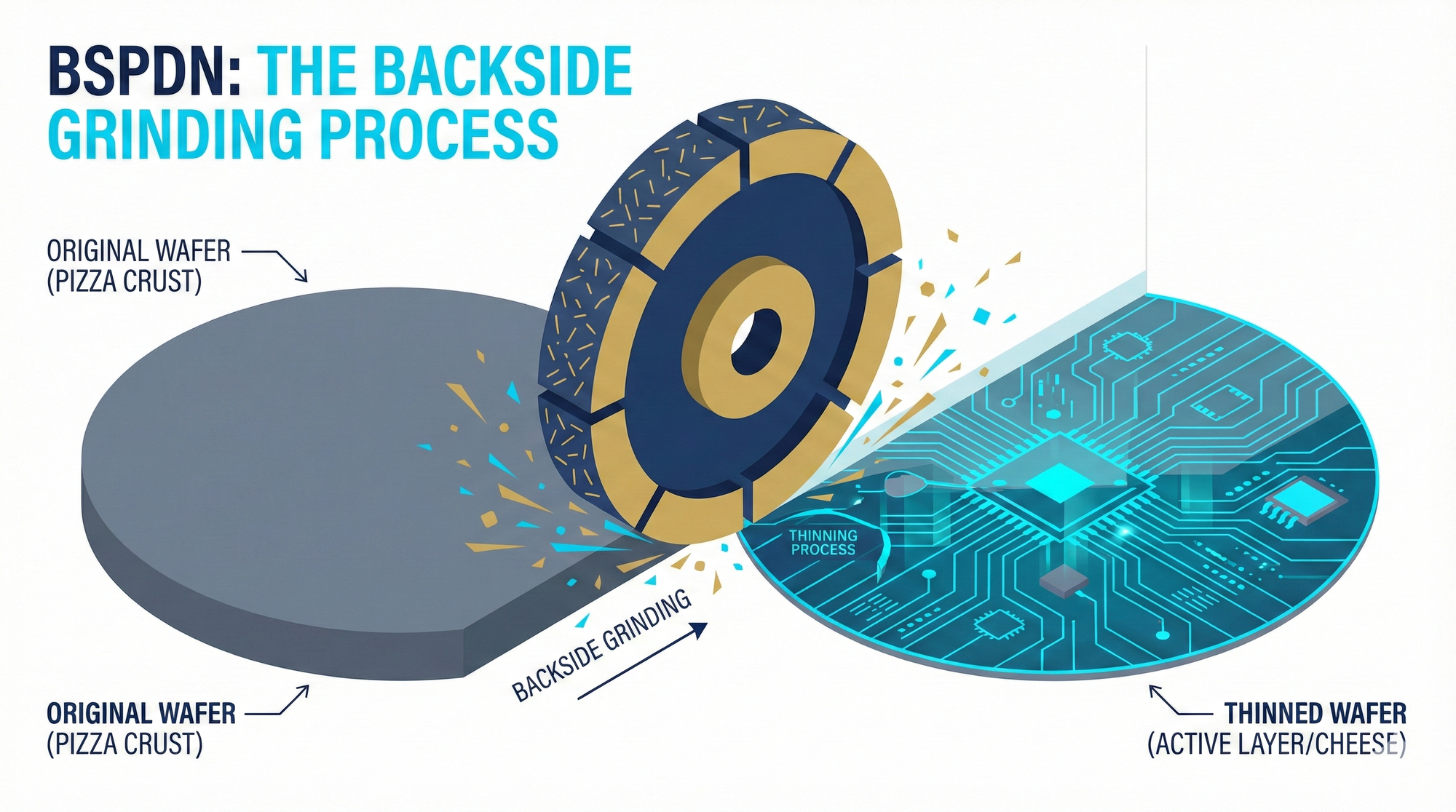
Before we move the power delivery lines to the backside, we must first confront an utterly absurd historical legacy issue in semiconductors: "That thick, useless pizza crust layer."
A standard 12-inch (300mm) silicon wafer has a thickness of approximately 775 micrometers (µm).
However, the "Active Layer" actually used for carving transistors and performing complex computations is only 1 to 2 micrometers thick on the surface. The remaining more than 770 micrometers are entirely pure silicon substrate (Substrate), used solely for robotic arms to "grip" and provide physical support.
It's like the extremely thick, hard crust beneath a pizza, having no electrical function itself.
The core manufacturing logic of BSPDN (Backside Power Delivery Network) sounds like a madman's ravings: "Grind away this useless crust layer, which accounts for 99% of the volume, and then connect the power lines directly to the back of the cheese (transistors)."
This is an extreme, "gut-wrenching" surgery on the wafer, divided into four critical stages:
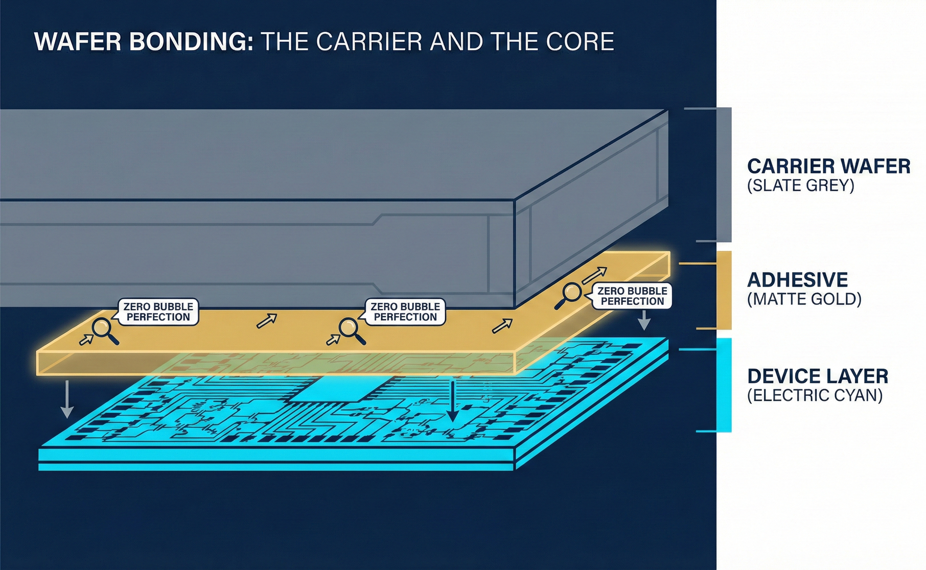
🥪 Step One: Temporary Bonding — The Fragile Stand-in
Mission: To provide a physical skeleton for the ultrathin wafer.
Core Equipment: EV Group (Austria), Tokyo Electron (TEL) (Japan), SUSS MicroTec (Germany).
When we prepare to grind a 775-micrometer wafer down to just a few micrometers, this originally rigid silicon wafer will become like a "wet tissue." With just a slight breeze or a gentle touch from a robotic arm, it will instantly curl and shatter. Therefore, before beginning the process, we must find a strong "stand-in" to support it.
Extreme Process Logic:
- Take a completely blank, rigid Carrier Wafer (usually glass or bulk silicon).
- Apply a layer of extremely specialized Temporary Adhesive onto it.
- Firmly bond the wafer, which already has its front-side transistors and signal lines fabricated (face down), to the carrier.
💡 Investor-Friendly Analogy: Nanoscale Screen Protector
This is like needing to apply a piece of reinforced glass to the front of an extremely fragile century-old painting to secure it before performing restoration work on its back.
Technical Difficulty: The adhesive must be applied "absolutely uniformly." If even a micron-sized air bubble is trapped in between, during the subsequent aggressive grinding, the wafer will experience stress concentration at the bubble and instantly burst. Even more challenging is "Debonding" — after all backside processes are completed, the carrier must be able to be detached "without damage or residue" using lasers or UV light. This demands an extremely stringent level of formulation from chemical material suppliers.
🚜 Step Two: Backside Grinding — The Brutal Art of Thinning
Mission: Grind away 99% of the silicon substrate.
Core Equipment: DISCO (Japan).
Dominant Position: DISCO holds a near-absolute monopolistic position in the wafer dicing and grinding sector (with a market share as high as 70% to 80%).
This is the most aggressive, yet also the most precise, step in the entire BSPDN process. DISCO's equipment will perform relentless cutting on this inverted wafer.
Extreme Process Logic:
- Coarse Grind: Using a coarse grinding wheel embedded with diamond particles, rapidly grind away most of the silicon substrate at extremely high rotation speeds, much like planing wood (reducing the thickness from 775 micrometers instantly to 50 micrometers).
- Fine Grind: Switch to an ultra-fine grinding wheel, reduce speed, and slowly grind down to just a few micrometers.
- CMP (Chemical Mechanical Planarization): Calling upon our old friend, the CMP equipment, which we mentioned in 2-5-3. Using chemical slurries and polishing pads, the wafer's backside is polished to a mirror-like flatness. Extreme Target: The final silicon thickness may be as thin as 500 nanometers (0.5µm) or even thinner!
💡 Investor-Friendly Analogy: Grinding a Mattress Flat from Underneath
Imagine you are soundly sleeping on a 100-centimeter thick spring mattress. DISCO's mission is to: start grinding upwards from the bottom of the bed, thinning the mattress until only 0.1 centimeters remain (the thickness of just a bedsheet). Furthermore, during the grinding process, the bedsheet must absolutely not be torn, nor should you (the transistors) sleeping on it feel any vibration or high temperature, otherwise the transistors will be damaged.
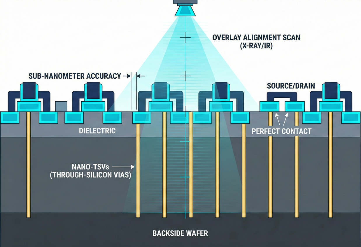
⛏️ Step Three: Nano-Through-Silicon Via (Nano-TSV) — Blindly Drilled Underground Passages
Mission: Drill holes to find contact points.
Core Equipment: ASML / KLA (Alignment and Overlay), Lam Research (Deep Hole Etching), Applied Materials (Metal Deposition).
Now that the wafer's backside has been ground down (leaving only a thin film), the next step is to drill holes from the backside to locate the contact points of the front-side transistors.
Extreme Process Logic:
- Lithography Overlay: This is the biggest nightmare. Because the chip has been flipped, ASML's lithography machines cannot see the alignment marks originally drawn on the front side! ASML and KLA must activate "infrared (IR) vision" to penetrate that 500-nanometer silicon layer and precisely align with the front-side coordinates in a vast sea of nothing.
- Extreme Etching (Nano-TSV Etching): Lam Research's plasma etchers dig aggressively downwards. Note that this is tens of times finer than traditional TSVs (Through-Silicon Vias) used in advanced packaging, belonging to the "nanoscale (Nano-TSV)" category. The drill must precisely reach the Source/Drain of the transistors and then instantly stop; digging just 1 nanometer too deep would perforate and scrap the chip.
💡 Investor-Friendly Analogy: Blind Archaeological Excavation
It's like digging upwards from the basement of a house. Without X-ray vision, you can only rely on faint signals from instruments to precisely dig through the wall of the first-floor living room to find an "outlet socket" and connect wires to it. Digging off-course would destroy the entire house's electrical system.
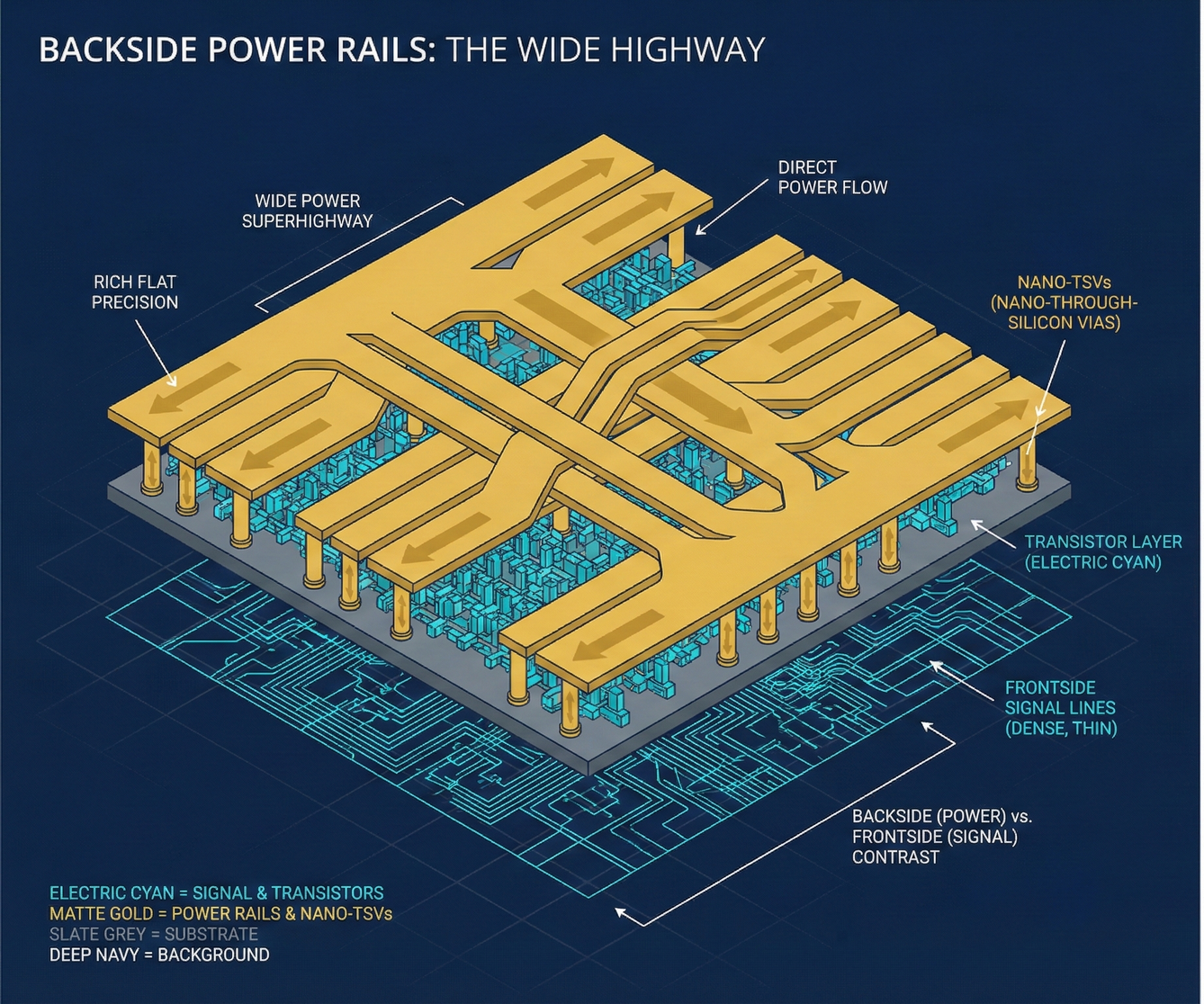
⚡ Step Four: Backside Routing — Laying Super Power Rails
Mission: Laying large, low-resistance "water pipes."
Core Equipment: Applied Materials (PVD / CVD Low-Temperature Metal Deposition).
Now that the backside silicon substrate has been hollowed out and successful underground passages to the transistors have been drilled, the final step is to lay ultra-thick, ultra-wide power metal lines on the vast open space of the backside.
Critical Constraint: Low-Temperature Processing.
At this point, the front side is already covered with delicate copper interconnects and insulation layers. If the temperature during metal growth on the backside is too high (exceeding 400°C), the copper lines on the front side will melt or undergo chemical diffusion. Therefore, Applied Materials must use extremely expensive low-temperature deposition technology to slowly and safely fill the backside with Ruthenium or copper.
Final Result: The backside power lines can be made as wide as a ten-lane highway! Resistance is significantly reduced, and the IR Drop (voltage drop) nightmare that has plagued the semiconductor industry for years completely vanishes at this moment.
📊 2-7-2 Strategic Summary: BSPDN Arms Dealer Power Map
Sir, Backside Power Delivery Network (BSPDN) is not just the ultimate victory for TSMC's A16 and Intel's 18A in terms of PPA (Power, Performance, Area); it's also a grand feast for these semiconductor equipment manufacturers. Every additional process step of "flipping, grinding, and drilling" means hundreds of billions in equipment procurement orders.
| Step | Core Process | Physical Challenge | Absolute Dominator (Ticker) | Wall Street Investment Keywords |
| 1. Bonding | Carrier Bonding | Bubble control, perfect flatness, damage-free debonding | EV Group (Austria, private), TEL | Equipment demand highly overlaps with CoWoS packaging, order visibility extremely high. |
| 2. Grinding | Backside Grinding | Nanoscale extreme thinning, vibration control | DISCO (6146.JP) | 🔥 Absolute leader and biggest dark horse. Benefits from both BSPDN and CoWoS. |
| 3. Alignment | IR Litho Overlay | Blind overlay alignment after flip (nanometer-level error) | ASML, KLA (KLAC) | Surging demand for dual-side lithography machines and high-end infrared inspection machines. |
| 4. Etching | Nano-TSV Etch | High aspect ratio drilling, atomic-level precision stopping | Lam Research (LRCX) | Etching steps and complexity increase exponentially again. |
| 5. Deposition | Backside Metal | Low-temperature process (avoid high temperature damage to front-side metal) | Applied Materials (AMAT) | Backside metal layer is a brand new blue ocean market; deposition equipment demand doubles. |
💡 Ultimate Insight: DISCO's Re-rating
In this list, Japan's DISCO is the biggest strategic dark horse.
For the past decade, Wall Street has viewed DISCO merely as a supplier of consumables and equipment for "back-end packaging (dicing wafers into small chips)," giving it a relatively low price-to-earnings ratio. However, with the advent of BSPDN, DISCO's grinding technology has officially entered the most critical and expensive "front-end process" of chip manufacturing. To grind a wafer down to 500 nanometers without damaging the transistors is something almost only DISCO can achieve worldwide. This provides DISCO with a strong foundation to redefine its market valuation (re-rating).
In-depth Research · Quantitative Perspective
Want to gain more insights into semiconductor quantitative research?
【Insight Subscription Plan】Break Free from Retail Investor Mindset: Build Your Alpha Trading System with "Quantitative Chips" and "Consensus Data"EDGE Semiconductor Research
📍 Series Map — Navigate the Complete EDGE Semiconductor Research →


