Foreword: Underground Secret Passages, The Last Mile Decision
Sir, in the previous chapter, we established the macro strategy for BSPDN (Backside Power Delivery Network): to alleviate the crowded front side of the chip, we must move all the thick and noisy power lines to the backside of the wafer.
This sounds like a perfect utopia, but when engineers actually enter the cleanroom, preparing to drill holes on the backside of the silicon wafer, the devil lies in the tiniest physical details. This detail is: "Where exactly should the power lines routed from the backside connect to the transistor?"
💡 Investor's Analogy: Underground Plumbing for a Building Imagine you are the chief engineer of a premium office building (chip). You have successfully buried the massive main water pipe (power) into the basement (wafer backside). Now, you need to deliver water to the employees (transistors) in the first-floor offices. You have two construction blueprints: Construction Method A (Intel): Pull the underground pipe upwards, through the first-floor floor, over the employees' heads, connect it to the first-floor "ceiling," and then run a small pipe down from the ceiling to the faucet. Construction Method B (TSMC): Pull the underground pipe upwards, directly and precisely align it, connecting it firmly to the "exact underside (under the floor)" of the first-floor faucet.
This seemingly minor difference in routing hides vastly different business calculations, risk tolerances, and relentless pursuit of future PPA (Performance/Power/Area) limits by Intel and TSMC.
🏎️ Chapter One: Intel PowerVia — The Smart First Mover and De-risking
Codename: Intel 20A / 18A (Mass production expected 2024-2025) Guiding Strategic Principle: Seize the narrative, extreme de-risking.
We must first understand Intel's current situation. The former CEO left a mess, and current CEO Pat Gelsinger announced the audacious slogan of "five process nodes in four years." Intel was late to both the FinFET and EUV generations, and it is desperate to reclaim the title of "technology leader" in the next (angstrom-era) generation.
Therefore, Intel is extremely aggressive with BSPDN technology, eager to launch its own backside power delivery technology — PowerVia — by 2024-2025. But to ensure this gamble doesn't turn into a disaster due to yield collapse, Intel's engineers made a very clever, yet relatively conservative, compromise in the physical architecture.
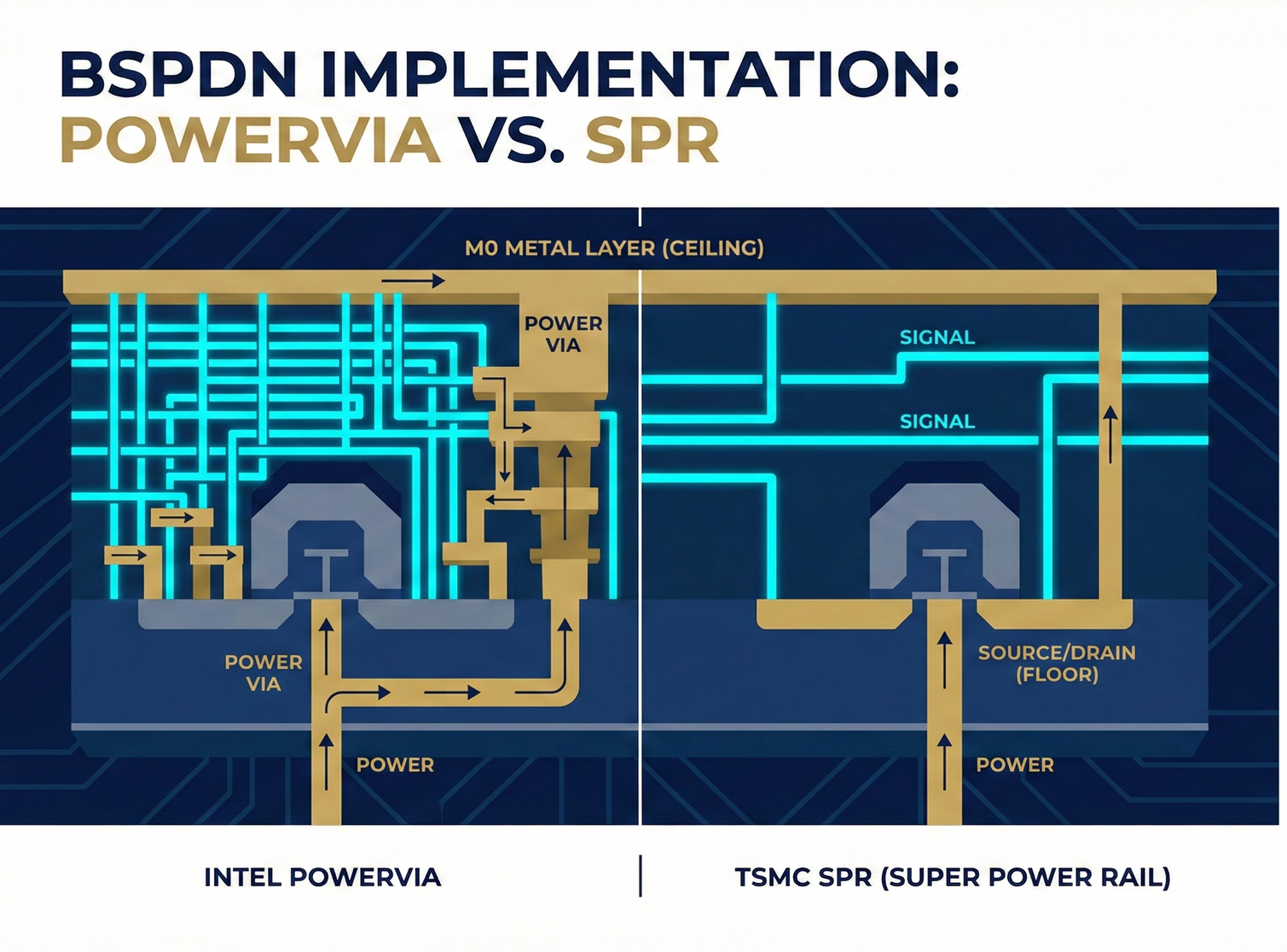
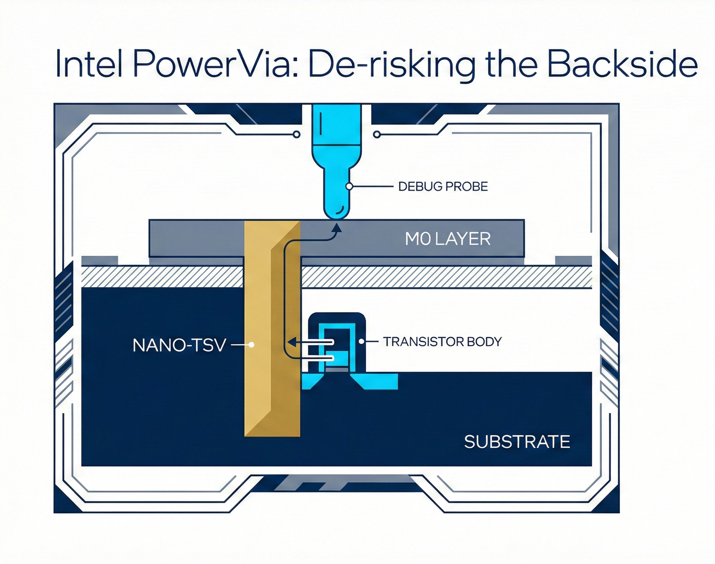
1. Technical Path: Connecting to M0 (Metal Layer 0)
Intel's PowerVia adopts the aforementioned "Construction Method A."
- Structural Details: Intel uses Nano-TSV (nanoscale Through-Silicon Via) technology to drill upwards from the backside of the wafer. However, this hole does not directly touch the transistor's most sensitive core body.
- This nanosized via penetrates through the thick silicon substrate, goes around the transistor, pushing upwards, and finally connects to the M0 metal layer on the front side of the chip (which is the "ceiling" layer directly above the transistor).
- Once power reaches M0, it is then transmitted downwards to the transistor's Source and Drain via the fine metal lines on the front side.
💡 Investor's Analogy: The "Ceiling Route" Diversion Tactic Although the power lines majestically took the back entrance (wafer backside), avoiding the need to crowd the elevators with high-level signal lines. However, its "last mile" still routes back to the front side's lowest metal layer (M0).
2. The Double-Edged Sword of Business and Physics (Pros and Cons)
Why did Intel choose this approach? It's filled with survival-driven actuarial calculations.
- Pro One: Extremely Debug-Friendly This is Intel's most valued point. Chips inevitably encounter errors (bugs) during manufacturing, requiring engineers to use electron microscopes to check voltage correctness. If all power lines were buried immovably at the backside bottom, engineers would be like blind men unable to debug. PowerVia, by ultimately connecting power back to the front-side M0, retains test nodes on the front. For a company urgently needing to improve yield and regain customer confidence, this is a life-or-death safety play.
- Pro Two: Manufacturing Simplicity The transistor's Source/Drain is the most fragile and sensitive part of the entire chip (especially when transitioning to a brand new RibbonFET / GAA architecture). Intel's solution cleverly "bypasses" this part, avoiding direct contact, thereby significantly reducing the risk of physical damage.
- Fatal Con: Compromised Area Scaling There's no such thing as a free lunch. Since you ultimately route power back to the front-side M0 layer, this means that the M0 layer must still retain significant space for power lines. When chip designers draw standard cells, they will find that because M0 is occupied by power lines, the cell height cannot be further aggressively compressed. In other words, Intel's PowerVia indeed solves the IR Drop problem, improving performance; but it does not achieve ultimate results in "reducing chip area and lowering costs."
This is a perfect strategic compromise made for "Time-to-Market" and "ensuring yield." Intel used this to declare to Wall Street: "Look, we were the first to implement backside power delivery!"
But at this moment, TSMC executives in Hsinchu, Taiwan, looking at this architecture, revealed a cold smile. TSMC was waiting, waiting for an opportunity to deliver a fatal blow.
🦖 Chapter Two: TSMC Super Power Rail (SPR) — The Ultimate Performance-Driven Annihilation
Codename: A16 (Mass production expected H2 2026)
Guiding Strategic Principle: Performance above all, delivering an uncompromising PPA (Performance/Power/Area) advantage to crush competitors.
TSMC's decision-making logic stands in stark contrast to Intel's.
TSMC decided to "temporarily not introduce" backside power delivery in the N2 (2nm) generation in 2025. This caused an uproar on Wall Street at the time, with some foreign investment firms even publishing reports questioning whether TSMC was falling behind technologically.
But TSMC's calculations were more precise than anyone else's. It knew that customers didn't want a "gimmicky presentation," but rather the tangible physical limits that "could make chip areas smaller and computing power higher." Therefore, TSMC chose to lie in wait, only introducing BSPDN in one fell swoop with the A16 (1.6nm) process in the second half of 2026.
The move it plans to make is called SPR (Super Power Rail).
1. Technical Path: Direct Connection to Source/Drain
TSMC adopted the most aggressive, yet also the most perfect, "Construction Method B."
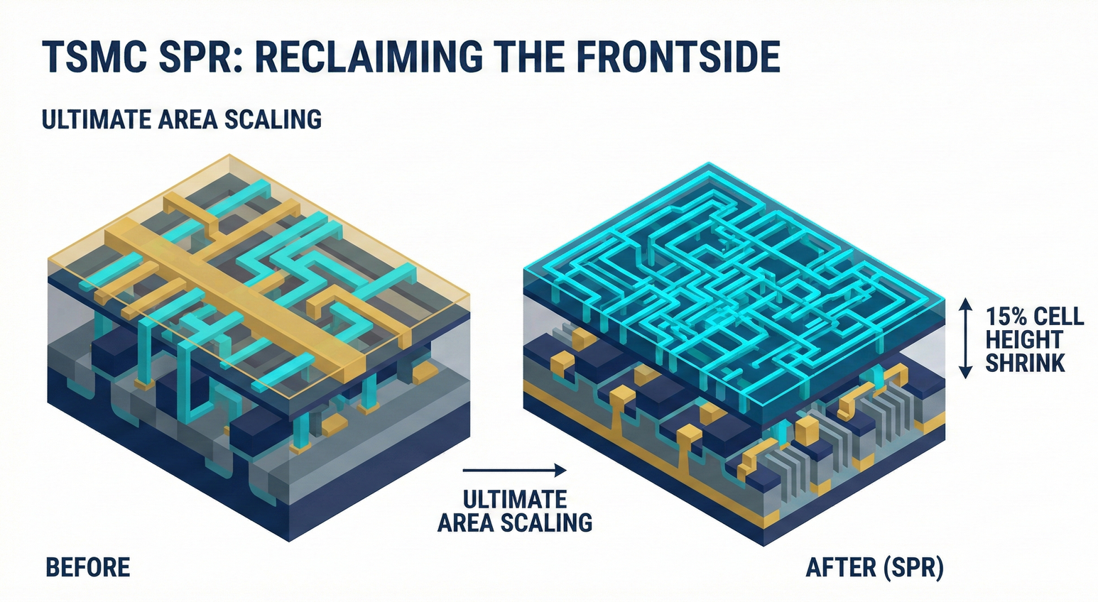
- Structural Details: SPR completely abandons Intel's compromised approach of routing to the "ceiling" (M0). After penetrating through the residual silicon substrate, TSMC's backside power lines directly and precisely connect to the Source and Drain contact points buried at the very bottom of the transistor.
- Completely Bypassing the Front Side: The front-side M0 metal layer no longer needs to reserve any space for power lines; it is 100% completely freed up for signal lines exclusively.
💡 Investor's Analogy: The "Floor Route" Direct Confrontation
The main water pipe from the basement is pulled upwards, completely bypassing the first-floor corridor or ceiling, and is directly and firmly welded to the "exact underside (under the floor)" of the first-floor faucet. This is the "absolute shortest path" physically possible.
2. The Double-Edged Sword of Business and Physics (Pros and Cons)
For this "absolute shortest path," TSMC undertook hellish manufacturing risks, but it also gained super benefits that customers cannot refuse.
- Pro One: Ultimate Area Scaling This is the core reason why Apple and NVIDIA are willing to wait two years for TSMC. Because the front-side M0 is completely clear, chip designers can unreservedly flatten and densely pack standard cells. Strategic Result: For the same computing power, SPR can further reduce the total chip area by 10% to 15%. For Apple, this means it can pack billions more AI Neural Processing Units (NPUs) into an iPhone chip of the same size; or save tens of millions of dollars in silicon wafer costs when producing the same number of chips.
- Pro Two: Lowest IR Drop The shortest path means that unnecessary voltage loss during transmission is minimized, transistors receive the fullest power, and clock speeds can be pushed to the extreme.
- Fatal Con: Hellish Manufacturing Difficulty and Thermal Nightmare
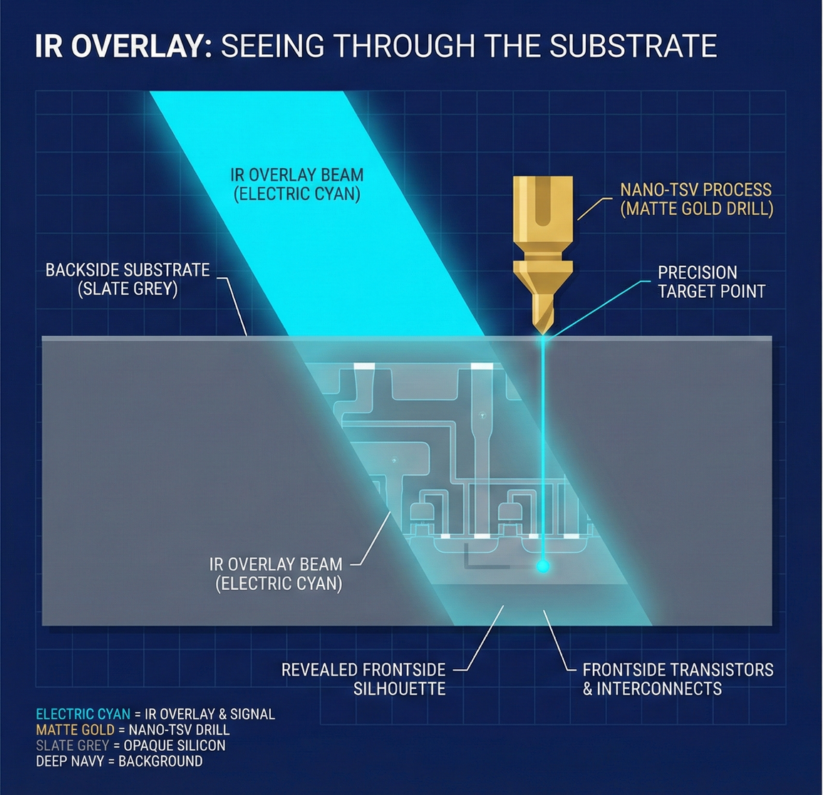
- Alignment Hell: On the "backside" of the wafer, one must blindly drill a nanosized deep hole, and moreover, precisely hit the extremely tiny Source/Drain contact point at the bottom of the front-side transistor. Even a slight tremor of 1 nanometer off-target will completely destroy the transistor's channel.
- Thermal Nightmare: Previously, waste heat could dissipate through the silicon substrate. Now, the silicon substrate is ground away, and the backside is filled with heat-generating power lines. Heat is trapped in the middle with "nowhere to escape," which places extreme demands on advanced packaging thermal materials.
⚔️ Chapter Three: Supply Chain Arms Race — The Golden Age for Equipment Manufacturers
Whether it's Intel's PowerVia or TSMC's SPR, for semiconductor equipment manufacturers (the "arms dealers"), it's a carnival. Each "dissection" of an architecture means frantic procurement of new machinery.
1. The Life-or-Death Battle of Inspection and Metrology (KLA / ASML)
In 2-5-4, we discussed KLA and ASML's dominance in metrology. Now, backside power delivery presents them with their toughest challenge: Overlay alignment.
- Intel's Challenge (Difficulty: Hard): Intel only needs to align with the front-side M0 metal lines. Because M0 lines are relatively wider, the tolerance for error is slightly larger.
- TSMC's Challenge (Difficulty: Nightmare): TSMC's drill must precisely hit the extremely tiny Source contact points.
- The Equipment Suppliers' Solution: To "see" the front-side contact points from the opaque backside of the silicon wafer, ASML and KLA must comprehensively upgrade their overlay machines, introducing ultra-powerful Infrared (IR) penetration metrology technology. Whoever can sell the most precise IR alignment machines will capture the largest inspection orders for the A16 process.
2. The Devil of Thinning Limits (DISCO)
- To route power from the backside, you cannot retain the original 700-micrometer thick silicon wafer (drills simply cannot penetrate that deep).
- You must flip this incredibly fragile 12-inch wafer onto a grinding machine and aggressively thin it down to a thickness of several micrometers (tens of times thinner than a human hair).
- Because TSMC's SPR solution requires deeper buried contact points, the wafer must be thinned even more than for Intel's! This has brought a huge order to the Japanese grinding equipment giant DISCO. DISCO must provide extremely stable CMP (Chemical Mechanical Planarization) machines that will not scratch or damage the nanosized thin wafers.
📊 2-7-3 Strategic Summary: The Century Showdown of Face vs. Substance
Sir, the wargame simulation and final predictions for this battle, which will determine semiconductor supremacy from 2025-2027, are as follows:
| Feature Comparison | Intel PowerVia | TSMC Super Power Rail (SPR) |
| Estimated Mass Production Time | 2025 (Intel 18A) | H2 2026 (TSMC A16) |
| Backside Connection Point | M0 Metal Layer (Front-side Bottom "Ceiling") | Source/Drain (Transistor's Very Bottom "Floor") |
| Area Scaling Advantage | Moderate (M0 still occupied by power) | Excellent (Front-side M0 completely freed for signals) |
| Manufacturing & Alignment Risk | Medium-High (Debug-friendly, larger tolerance) | Extremely High (Blind alignment, slight deviation leads to scrap) |
| Core Strategic Significance | Speed. Prove technological competitiveness, gain PR victory and government subsidies. | Victory. Pursue absolute physical limits, provide clients with strongest PPA to crush competitors. |
Ultimate Strategic Assessment:
- Intel will win "face" (perception/image): Intel has an excellent chance to be the first to issue a global press release by late 2024 to 2025, announcing mass production of BSPDN, and publicly proclaiming "Intel's power delivery architecture leads TSMC by a full two years!" This is critically important for Pat Gelsinger, as it can significantly boost Intel's subdued stock price and secure the maximum subsidies under the U.S. CHIPS Act.
- TSMC will win "substance" (reality/practicality): TSMC may appear to be a step behind, but it deeply understands the brutal rules of the high-end chip market. Giants like Apple and NVIDIA truly care about absolute advantages in chip computing power and cost. Although the A16 SPR architecture is difficult to produce, once it is released, it can pack in more transistors and deliver stronger computing power. Customers' actions speak louder than words; they will quietly wait for TSMC for that 15% area reduction.
In-depth Research · Quantitative Perspective
Want more insights from semiconductor quantitative research?
【Insight Subscription Plan】Bid Farewell to Retail Investor Mindset: Build Your Alpha Trading System with "Quantitative Chips" and "Consensus Data"EDGE Semiconductor Research
📍 Series Map — Navigate the Complete EDGE Semiconductor Research →


