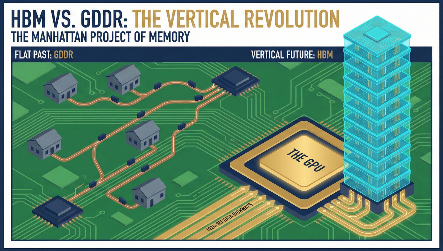
Preface: Urban Sprawl and the Dead End of GDDR
After pushing the computing power of TSMC-manufactured GPUs to their limits, we encountered the "compute famine" mentioned in 3-0. To address this issue, we must first look at how graphics cards have designed memory over the past few decades.
In the past (and even in most gaming PCs today), graphics cards were surrounded by a circle of black chips called GDDR (e.g., GDDR6).
- Physical Structure: Suburban Bungalows. GDDR chips are like single-story bungalows, laid flat and scattered across the green PCB motherboard. If the GPU (city center) needs data from these bungalows, it must transmit it via copper traces (highways) within the PCB.
Why did the GDDR "bungalow" model completely collapse in the AI era?
- Limits of Footprint: The area of a server motherboard is fixed. You can fit at most 12 or 24 GDDR chips next to the GPU; any more won't fit. AI models often require hundreds of gigabytes, making bungalows simply insufficient.
- Excessively Long Commute Paths: Signals traveling across long PCB traces are not only extremely power-intensive but also suffer from severe transmission latency.
- Severely Insufficient Lane Count (I/O Bandwidth): Each GDDR chip typically has only a 32-bit (32-lane) data path to the outside. This is sufficient for gaming, but for ChatGPT, it's a severe traffic jam.
The HBM Solution: Memory's Manhattan Project Since planar space is already exhausted, the only solution is to "build upwards."
- Structure: Abandoning bungalows, 8, 12, or even 16 layers of DRAM chips are "vertically stacked" to form a sugar-cube-sized three-dimensional block, which we call HBM (High Bandwidth Memory).
💡 Investor-Friendly Analogy: From Bungalows to Skyscrapers HBM is not just a 12-story skyscraper; it also brings two revolutionary changes:
- Ultra-Wide Bandwidth: Each HBM skyscraper has a super channel at its base with up to 1024-bit (1024 lanes). When an NVIDIA H100 is surrounded by 6 HBM3 chips, its total bandwidth reaches an astonishing 3.35 TB/s.
- Extremely Short Path: Through CoWoS advanced packaging, which we will discuss later, this skyscraper is directly "adhered" next to the GPU, shortening the commute distance between them from several centimeters to mere micrometers.
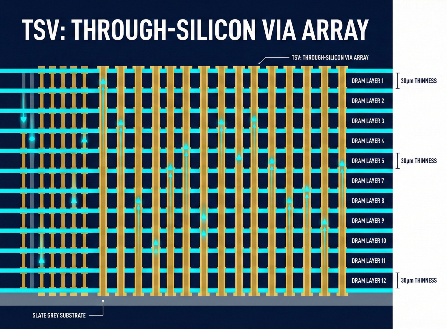
🏗️ Chapter One: TSV (Through-Silicon Via) —— The Nano-Elevator Inside the Chip
Now that we've stacked 12 DRAM chips into a skyscraper, a fatal physical problem arises: "How does data on the 12th floor get to the 1st floor?" You can't run external wires (because there's no space on the chip's edge). Your only option is to "drill wells" inside the building, creating nano-elevators that go straight to the basement.
1. Drilling & Plating
- Core Technology: TSV (Through-Silicon Via) Engineers must use Lam Research's deep-hole etching machines to create thousands of extremely tiny, vertical holes penetrating the silicon wafer on each fragile DRAM chip. Then, these holes are filled with conductive copper pillars.
- Insane Density: An HBM3 contains over 5,000 TSV channels. Imagine precisely drilling 5,000 holes on 12 sheets of paper and then perfectly aligning them. If even one copper pillar is misaligned, the entire HBM chip is scrapped.
2. Limits of Thinning
- Because HBM has strict industrial standards for its total height (if stacked too high, the heatsink next to the GPU won't fit flat). Therefore, when stacking 12 layers (12Hi) or even 16 layers, each DRAM chip must be thinned to be thinner than paper.
- Extreme Data Point: Each wafer must be thinned to a thickness of approximately 30 micrometers.
- Key Equipment: Here, we once again see the presence of Japanese grinding giant DISCO. The more layers in HBM, the better DISCO's grinding machines sell.
⚔️ Chapter Two: The Packaging War —— MR-MUF vs. TC-NCF (The Holy War of Adhesives)
Sir/Madam, next is the most exciting business battle in this report. Why did Samsung (South Korea), which has long dominated the memory industry with the world's largest market share, suffer such a crushing defeat in the HBM battle against long-time runner-up SK Hynix, even losing 100% of NVIDIA's initial H100 exclusive orders?
The answer doesn't lie in whose DRAM circuit design is better; victory or defeat was entirely determined by a "glue" war.
Bonding 12 chips, each thinner than paper and covered with 5,000 tiny copper pillars, is a hellish engineering task.
1. Samsung's Persistence: TC-NCF (Thermal Compression Non-Conductive Film)
This is a traditional process long used in the semiconductor industry, and it was the path Samsung initially adhered to.
- Method: A thin insulating film (NCF) is sandwiched between each layer of chips. Then, a high-temperature thermal compression bonder presses down firmly from above, compressing and bonding the copper pillars between the chips.
- Layman's Analogy: It's like applying double-sided tape. One layer of chip, one layer of double-sided tape, then press firmly.
- Fatal Flaws:
- Slow: Heating and pressing must be done "layer by layer," resulting in extremely low productivity.
- Prone to Cracking: To ensure all 5,000 tiny copper pillars are electrically connected, the physical force applied is immense. For chips only 30 micrometers thick, this easily causes micro-cracks, leading to yield collapse.
- Poor Thermal Conductivity: This film (NCF) is essentially an insulator, offering very poor thermal conductivity.
2. SK Hynix's Decisive Blow: MR-MUF (Mass Reflow Molded Underfill) 🌟
SK Hynix engineers shrewdly realized that traditional double-sided tape processes could not handle stacks of 12 or more layers. They boldly abandoned the film and introduced an entirely new chemical magic.
- Method:
- First Stack: All 12 layers of chips are stacked first. Between the chips, only tiny solder balls (Microbumps) are used for temporary adhesion. At this point, there are "gaps" between the chips.
- Then Underfill: The entire stacked skyscraper is placed into a mold, and then a special liquid epoxy is injected. This high-tech liquid, like water, perfectly penetrates the tiny gaps between each chip layer via capillary action.
- Single Bake (Mass Reflow): It's sent into a large oven, heated to melt and solder the microbumps, and simultaneously cure the liquid resin. One-shot completion!
- Layman's Analogy: It's like building a house. First, the 12-story framework is erected with rebar (microbumps), then liquid ready-mix concrete (resin) is poured in from the top floor all at once. Once the concrete dries, the building is solid as a rock.
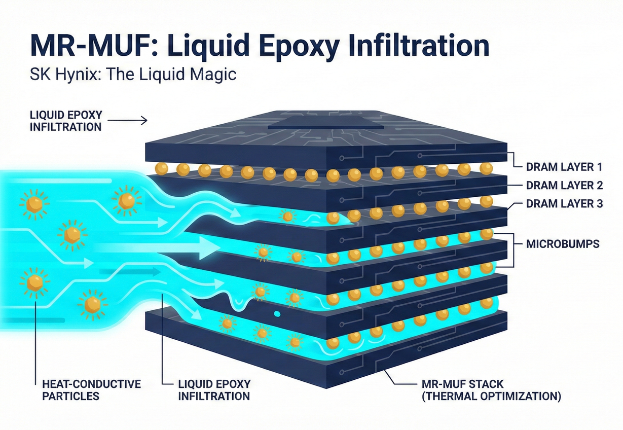
SK Hynix's Ultimate Key to Victory: Heat Dissipation! The reason MR-MUF delivered a decisive blow to Samsung was not just its "speed," but because SK Hynix incorporated a large amount of highly thermally conductive powder into this liquid encapsulant. NVIDIA's H100 is a power-hungry beast with terrifying heat generation. HBM is tightly coupled next to the GPU, and if heat dissipation is poor, the HBM will directly thermal throttle. SK Hynix's cured resin not only firmly protects the fragile chips like stone but also boasts thermal efficiency that far surpasses Samsung's film.
Outcome of the Battle: NVIDIA unhesitatingly chose SK Hynix for its superior heat dissipation and higher yield. SK Hynix consequently secured 100% of the initial HBM3 exclusive orders for H100, seeing both its profits and stock price skyrocket. In contrast, Samsung, despite urgently improving its TC-NCF technology afterward (claiming improved yield), found the lost time and trust difficult to recover. To this day, it struggles to secure the remaining scraps as a second supplier (Tier 2) in NVIDIA's supply chain.
🧱 Chapter Three: The Future of HBM4 —— Hybrid Bonding
Sir/Madam, we have now entered 2026, and the first year of HBM4 mass production has officially begun.
NVIDIA's next-generation flagship GPUs (such as the Rubin architecture) demand memory bandwidth and capacity that have reached unimaginable levels. To solve the capacity famine, HBM4 must forcibly increase the stack height of DRAM chips from 12 layers (12Hi) to 16 layers (16Hi) or even 20 layers.
At this point, a fatal physical ceiling has emerged: microbumps (the tiny solder balls mentioned in the previous article) are too large.
When stacking 16 layers of chips, if you still sandwich a solder ball between each layer, the "total height" of the entire skyscraper will severely exceed limits, making it impossible to fit into standard advanced packaging modules. What's worse, solder balls themselves have electrical resistance; signals passing through 16 layers of solder balls would cause latency and heat generation that would directly crash the system.
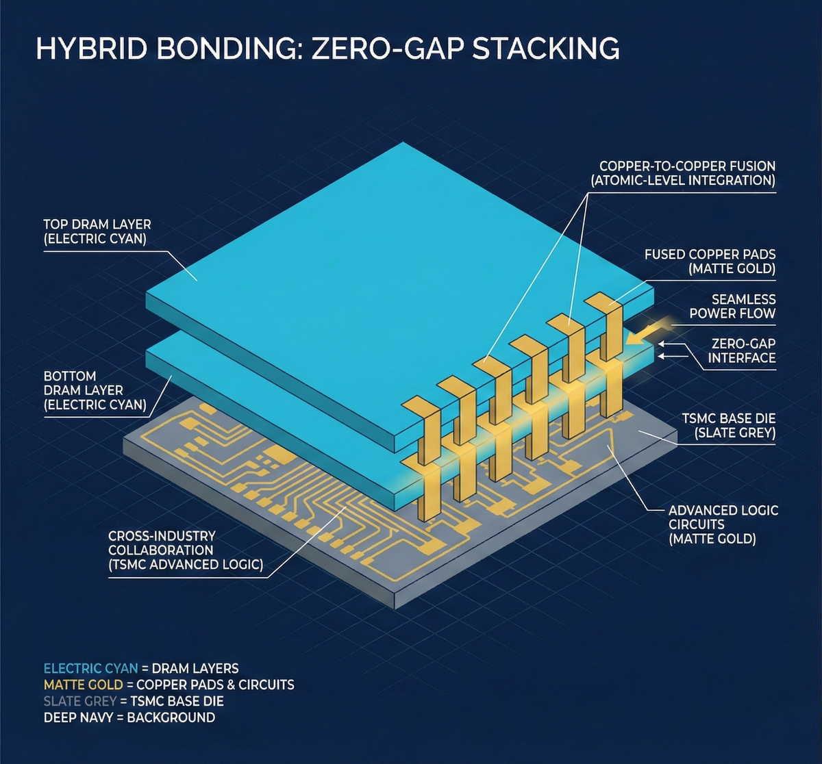
1. Copper-to-Copper Atomic-Level Fusion (Direct Bonding)
To resolve this height crisis, the semiconductor industry has brought forth the holy grail of packaging technology: Hybrid Bonding.
The essence of this technology is quite radical: "Since solder balls take up too much space, we'll just eliminate them."
- Physical Principle: Engineers use Chemical Mechanical Planarization (CMP) to polish the surfaces of two wafers, top and bottom, to be "super, absolutely, atomically flat." Then, without any adhesive or solder balls, the two wafers are directly bonded together.
- The Magic of Van der Waals Force: When two extremely flat copper contacts are brought close enough, quantum mechanical Van der Waals forces come into play. The copper atoms on both sides attract each other and directly "fuse" together, becoming a solid piece of copper.
💡 Investor-Friendly Analogy: Nano-Scale Ice Cube Fusion
Imagine taking two ice cubes with extremely flat surfaces from the freezer. When you press them tightly together, the water molecules at their contact surfaces recombine, and the two ice cubes eventually "grow into one large ice cube," with not even a single gap in between.
Advantages: The distance between chips becomes almost "zero." Thickness is drastically reduced, signal transmission is unimpeded, and electrical resistance and heat generation are minimized to their physical lowest points.
2. The Ultimate Player: TSMC's Strong Intervention
This "solder-ball-free" hybrid bonding technology has an extremely high barrier to entry. Currently, the most skilled practitioner on Earth is TSMC (Taiwan Semiconductor Manufacturing Company).
From HBM1 to HBM3e, the bottom-most chip responsible for controlling data ingress and egress was called the Base Die (logic control layer). Previously, this Base Die was manufactured by the memory companies themselves (SK Hynix, Samsung) using mature process nodes (around 2X nanometers).
However, with HBM4, due to the enormous data transmission volume, the Base Die must become extremely intelligent. It can no longer use old process nodes; it must upgrade to advanced process nodes of 12 nanometers or even 5 nanometers!
What does this mean? It means memory manufacturers simply cannot produce this bottom-most chip.
- Strategic Shift: Starting with HBM4, the most critical Base Die will be entirely manufactured by TSMC as a foundry. After TSMC produces the Base Die, it may even directly utilize its own Hybrid Bonding technology to help stack the DRAM chips on top.
- Outcome: TSMC will no longer merely be the "system assembler" that ultimately bonds the GPU and HBM together; it will deeply involve itself in HBM's "internal manufacturing process." In this memory war, TSMC has become the true kingmaker.
📊 3-1 Strategic Summary: The Memory Power Rankings and Arms Dealers Directory
Sir/Madam, HBM is currently the fattest and most astonishingly profitable segment in the semiconductor industry. This strategic summary table outlines the current power map of the memory market and the arms dealers quietly raking in profits behind the scenes:
💡 Investors' Ultimate Keywords (The Arms Dealers)
In times of war, those who sell shovels always profit the most. Beyond focusing on TSMC and SK Hynix, the real beneficiaries of this HBM boom are the hidden equipment supply chains behind them:
- Hanmi Semiconductor (South Korean stock): It is the most important contributor behind SK Hynix. It specializes in providing TC Bonders (thermal compression bonders) for precisely pressing chips. As SK Hynix massively expanded its HBM production capacity, Hanmi's orders surged, and its stock price experienced an epic rise over the past two years.
- DISCO (Japanese stock): We mentioned it in the back-side power delivery (2-7-2) discussion. In the HBM domain, stacking 16 layers means each chip layer must undergo extreme grinding and thinning. HBM's demand for DISCO's grinding machines is more than 8 times that of traditional GDDR memory.
- Taiwan's "Special Forces" (K&S / Scientech / APT): Although Taiwan does not have its own major HBM memory manufacturer, Taiwanese companies have also gained a share in this packaging feast. HBM requires a large amount of wet process and baking equipment for underfilling, curing, and post-TSV drilling cleaning. Equipment suppliers led by Scientech (辛耘) and APT (弘塑) are closely following TSMC and the global expansion of advanced packaging, entering a golden period of explosive growth.
In-depth Research · Quantitative Perspective
Want to gain more insights into semiconductor quantitative research?
【Insight Subscription Plan】Break Free from Retail Investor Mindset: Build Your Alpha Trading System with "Quantitative Chips" and "Consensus Data"EDGE Semiconductor Research
📍 Series Map — Navigate the Complete EDGE Semiconductor Research →


