Foreword: From Crowded Bungalows to Reclaiming Space from the Sky
Sir, after examining how DRAM and HBM push their limits for "transmission speed," we now turn our attention to the other extreme of the memory world: NAND Flash (flash memory), responsible for "permanent data storage."
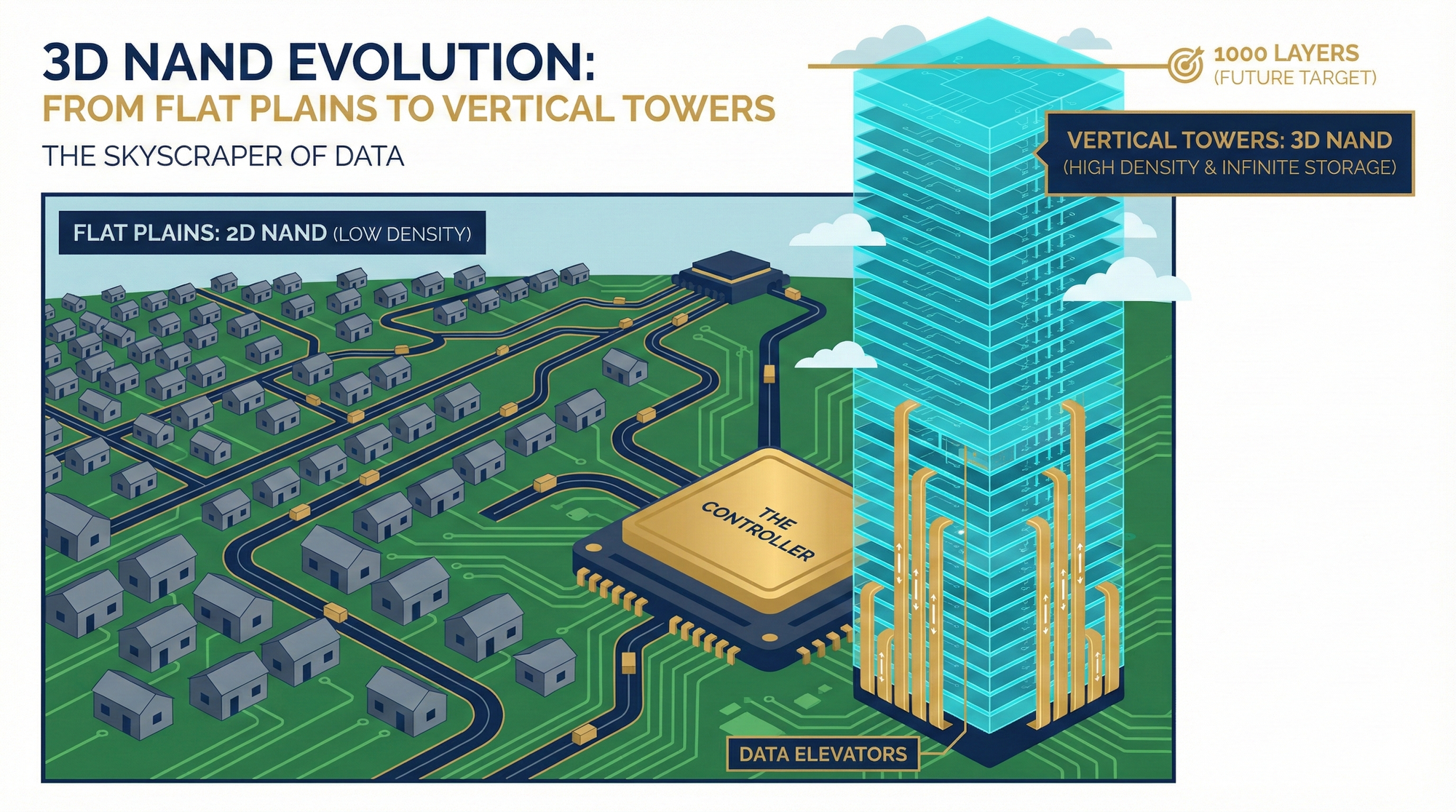
If DRAM is a mobile desk that can only temporarily store data, then NAND Flash is a large archive that never loses power. Before 2015, this archive was planar (2D Planar NAND), much like building an entire neighborhood of single-story bungalows on flat land.
However, as semiconductor scaling technology advanced to 15 nanometers, disaster struck the bungalow community. The 'rooms' (storage cells) became too small and too close together. The electrons used to record data began to interfere with each other and drift randomly (quantum tunneling and leakage effects). The capacity of planar NAND officially reached its physical limits.
The Birth of 3D NAND: Reclaiming Capacity from the Sky Since the land wasn't big enough and the rooms couldn't be shrunk further, engineers arrived at a simple and direct conclusion: “Then let's build skyscrapers upwards!”
- Structural Transformation: Major memory manufacturers stopped planar scaling and instead began to "vertically stack" memory cells.
- The Current Frenzy (2026 Perspective): We have rapidly progressed from 176-layer and 232-layer in 2022 to the current 9th/10th generation 3D NAND with over 300 layers. And the ultimate future goal for Samsung, Hynix, and Micron is to achieve an incredible 1000-layer mega-tower.
However, building this nano-skyscraper, the hardest part isn't "stacking" the layers, but rather how to "connect" them.
🏗️ Chapter One: The Layer Count War —— Lam Research's Absolute Dominance
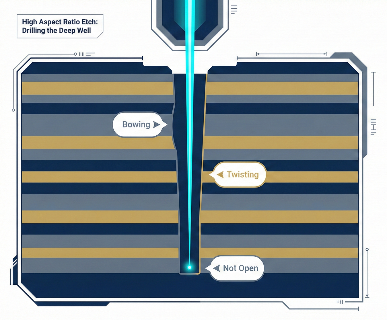
Sir, imagine this: after stacking 300 layers of extremely thin films alternately composed of oxides and nitrides (or polysilicon), this 'building' is a solid block with no elevators or conduits. You must precisely drill billions of deep holes downwards from the "top floor" of this 300-layer building to the ground floor foundation using a plasma drill, in order to insert electrodes and connect the 'rooms' on each layer.
This process is called High Aspect Ratio Etch (HAR Etch). This is the most expensive, time-consuming, and frustrating bottleneck in 3D NAND manufacturing.
1. The Physics Hell: High Aspect Ratio Etch
- Extreme Challenge: The depth of this hole is 70 to over 100 times its width.
💡 Investor-Friendly Analogy: Threading a Needle from the Top of Taipei 101 Imagine standing on the top floor of the 500-meter-tall Taipei 101, holding an extremely thin, long needle. You need to stab straight down and precisely pierce the center of a coin placed on the ground floor.
During this drilling process, if any of the following physical deformations occur, the entire chip is immediately scrapped:
- Bowing: Halfway through drilling, the middle of the hole widens, like a balloon.
- Twisting: When reaching the bottom, the hole becomes crooked, poking into the adjacent 'room'.
- Not open: The plasma drill loses momentum in the final layers and fails to penetrate to the bottom.
- Absolute Dominator: Lam Research (LRCX) In this extremely demanding "deep well excavation" process, US equipment giant Lam Research (LRCX) holds a near-monopolistic dominance. It is the only vendor globally that can reliably provide cryogenic plasma etching to handle the extreme challenge of drilling 300 layers. Core Investment Logic: The higher the number of layers in 3D NAND, the longer the drilling time required and the higher the failure rate. This means memory manufacturers must purchase more etching equipment from Lam Research. Lam is the quietest and most profitable winner in this layer count war.
2. Stacking & Xtacking: Compromises and Magic in Stacking
When buildings reach 300 layers, and even Lam Research's equipment cannot drill from the top floor to the ground floor in a single pass, humanity has to resort to physical compromises and architectural magic.
- Double-Deck / String Stacking: If drilling 300 layers at once results in misalignment, then do it twice! Manufacturers typically build the bottom 150 layers (Tier 1) and drill holes; then they build another 150 layers (Tier 2) on top and drill holes again. Finally, the upper and lower holes are perfectly aligned and connected. This effectively doubles the demand for equipment purchases.
- Xtacking (YMTC's Astonishing Technology): In traditional 3D NAND, in addition to the "rooms" (arrays) used for storage, a separate area must be reserved next to them for the "guardhouse" (CMOS logic circuits) responsible for management. This takes up a lot of space. Although China's Yangtze Memory Technologies Corp (YMTC) has been sanctioned by the US, they invented an industry-shocking technology called Xtacking: They focused on building 300 layers of "rooms" on one wafer, and on building the "guardhouse" on another wafer. Finally, these two wafers are precisely "hybrid bonded" together like a sandwich. This not only pushes area utilization to its limit but also compelled international giants like Samsung and Micron to adopt similar CMOS-under-Array (CuA) or wafer bonding concepts in their next-generation architectures.
👨👩👧👦 Chapter Two: The Tenant War —— The Necessary Evil of QLC
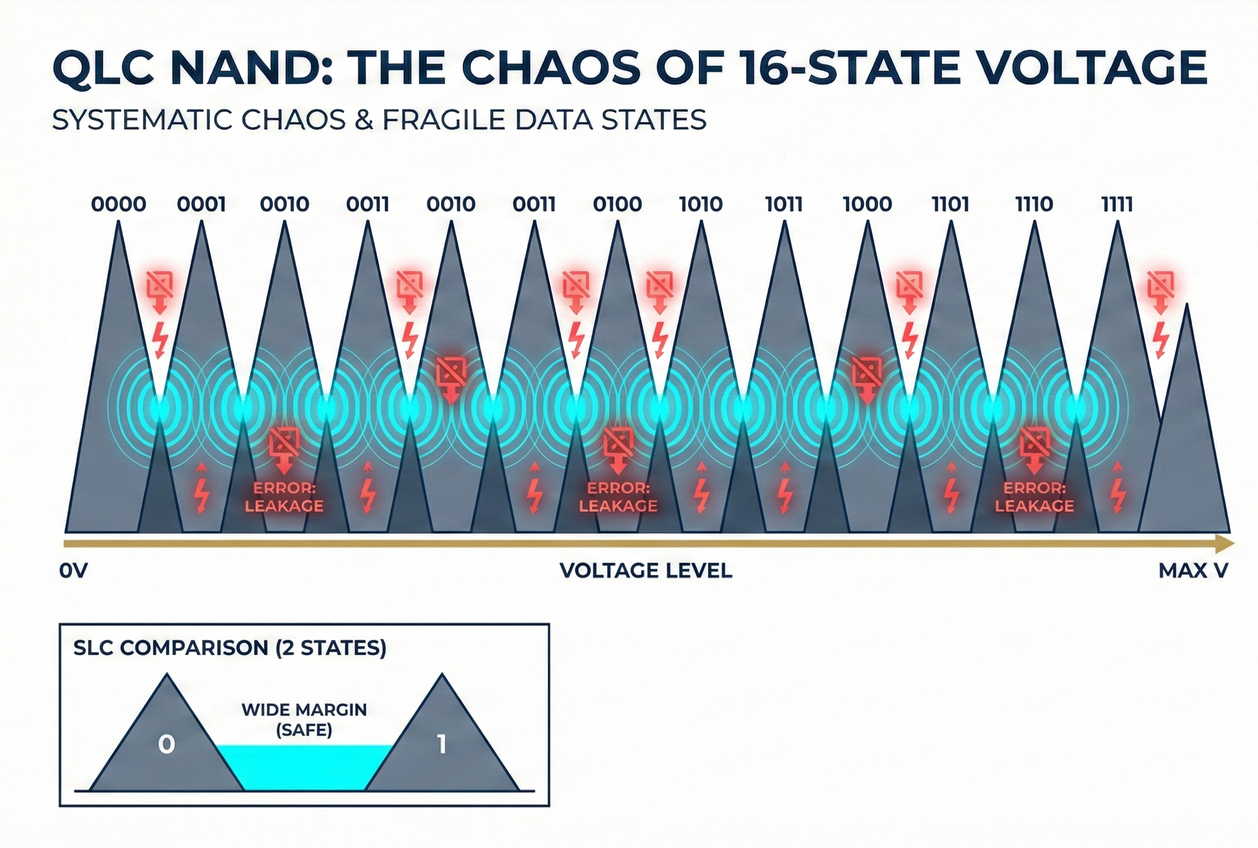
Sir, in the world of NAND Flash, we use the number of "electrons" to represent data (bits).
Each floor contains countless tiny "rooms" (memory cells). If we could only increase capacity by "building taller structures" (increasing layers), the cost would be prohibitively high. Engineers devised a clever solution: alter the design of the "rooms" to accommodate more "occupants" (bits).
This is the evolution of SLC, MLC, TLC, and QLC architectures commonly heard in the semiconductor industry.
1. Crowded Rooms (The Cell Density)
- SLC (1-bit): Premium Single Occupancy Room.
- The room only has two simplest states: "charged (1)" and "uncharged (0)" (2 voltage levels).
- Features: Ultra-fast, extremely durable (a single cell can endure up to 100,000 erase/write cycles), but since only one "occupant" resides in a room, the per-unit cost is exceptionally high.
- TLC (3-bit): Standard Triple Occupancy Room.
- This is also the mainstream specification currently found in our smartphones and laptops. With three "occupants" per room, the system must precisely distinguish between $2^3=8$ different voltage states.
- QLC (4-bit): Extreme Quad Occupancy Room (The Future Dominator).
- This is a physical disaster. To cram four bits of data into one room, the system must precisely delineate $2^4=16$ minute voltage levels within this extremely tiny space.
- Advantages: Unbeatable capacity! Offers 33% more storage space than TLC and has extremely low per-unit cost, making it a favorite for large data centers.
- Fatal Flaws: Short lifespan, extremely slow, highly prone to errors. Because the 16 voltage states are so close together, even a slight leakage (interference) from an adjacent "room" can cause the voltage representing "A" to drift and become "B", leading to data read errors (bad blocks). Furthermore, its lifespan is extremely short, capable of enduring only about 1,000 erase/write cycles.
2. Why Must AI Embrace Fragile QLC?
Given how poor QLC's physical characteristics are and how easily it can fail, why are Microsoft and Meta's AI servers currently aggressively purchasing Enterprise QLC SSDs?
Because AI's operational model perfectly conceals QLC's drawbacks while amplifying its advantages.
- Read/Write Characteristics of Warm Data: The massive datasets used for AI training have a characteristic of "write once, read ten thousand times." You write Wikipedia data to a hard drive, and you're unlikely to modify it again; instead, the GPU repeatedly reads it.
- Since frequent "writes (erases)" are not needed, the problem of QLC's short lifespan is effectively resolved. And in AI inference scenarios that demand extremely high capacity, low power consumption, and read speeds far superior to traditional hard disk drives (HDDs), QLC SSDs have become the perfect savior to replace HDDs.
🧠 Chapter Three: The Controller Chip —— The Magic that Turns Rotten into Remarkable
Sir, a critical question arises: given QLC's physically fragile nature and its propensity for read errors due to voltage drift, why do tech giants dare to entrust their invaluable AI databases to it?
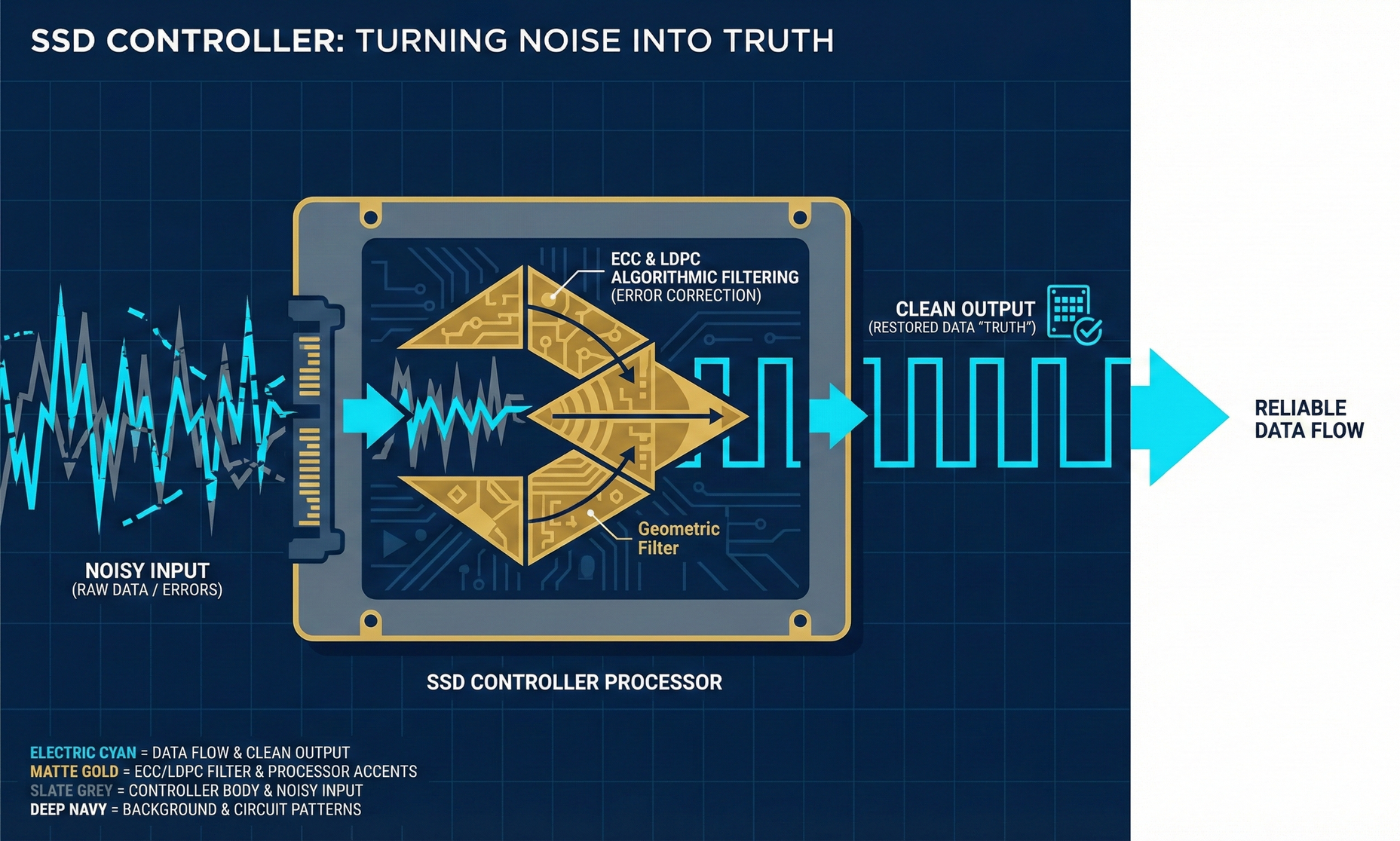
Because behind every SSD stands a highly intelligent, constantly busy "super steward" — the controller chip.
Here, Taiwan's Phison Electronics (8299.TW) and Silicon Motion Technology (SMI) control half of the global SSD "brains."
Without the powerful firmware written by these Taiwanese "stewards," QLC would simply be unrecognizable electronic waste.
1. ECC Error Correction Engine: Hearing the Truth Amidst Noise
- Scenario: Due to overcrowding of electrons in QLC, the signals they transmit are full of noise whenever the CPU requests data, much like trying to discern minute tonal differences in a noisy marketplace.
- Controller Chip's Magic: The chip incorporates a powerful LDPC (Low-Density Parity-Check) algorithm. It acts like a god-tier real-time interpreter, instantly using mathematical probability models to "deduce and automatically correct" the original correct data when reading confused and erroneous voltage signals.
- Conclusion: QLC's physical limits were surpassed long ago; it's the controller chip's powerful mathematical algorithms that forcefully pulled it back from the brink.
2. Wear Leveling: Ensuring Everyone Ages Together
- QLC "rooms" can only withstand 1,000 "cleanings" (erase/write cycles). If the system consistently writes new data to the same block, that block would quickly fail within days, rendering the entire drive useless.
- The controller chip acts like an actuary, silently recording and orchestrating the storage location of every piece of data in the background. It forces new data to occupy "unused new rooms," ensuring that hundreds of billions of "rooms" "age uniformly," thereby extending the lifespan of the entire QLC SSD to support enterprise-grade warranties (five years or more).
3. Phison's Nuclear Weapon: aiDAPTIV+ Strategy 🌟
Phison is not content with merely being a "hard drive manager"; they identified a major pain point: Current AI models are too large, and "poor" users (general small and medium-sized enterprises or studios) simply cannot afford top-tier servers equipped with 8 H100s and hundreds of GBs of HBM memory.
- Phison's 'Jailbreak' Thinking: Since SSDs have such large capacities, why not use them to "mimic brain memory"?
- Phison introduced its aiDAPTIV+ architecture: when GPU VRAM (such as HBM/GDDR) is insufficient, Phison's controller chip actively intervenes, segmenting vast AI model parameters and temporarily storing them in its high-end SSDs (used as swap extended memory).
- Strategic Significance: Although SSDs are slower than HBM, this solution enables a standard workstation costing only hundreds of thousands of New Taiwan Dollars to run colossal open-source models like 70B (70 billion parameters) that previously required multi-million-dollar servers! This has opened up a new goldmine for controller chip manufacturers in "edge AI computing."
📊 3-3 Strategic Summary: The Future of Storage —— Algorithms vs. Deep Wells
Sir, this strategic summary table distills the core battlegrounds of the global storage market for the next 5 years for you:
Conclusion:
- "Inflation" of Controller Chips: Because QLC is incredibly difficult to control, it requires immense computational power to run LDPC error correction algorithms. Future controller chips can no longer use cheap older processes; they must upgrade to 12nm or even 7nm to reduce power consumption. This will directly drive a significant increase in Phison's and SMI's ASP (Average Selling Price) and gross margins.
- The Long Twilight of HDDs: In the high-speed data floods of AI servers, the drawback of traditional hard disk drives (HDDs) having slow read speeds is infinitely magnified. While HDDs still hold a price advantage for "cold data" archiving, the widespread invasion of Enterprise QLC SSDs into AI servers is an irreversible trend.
In-depth Research · Quantitative Perspective
Want more semiconductor quantitative research insights?
【Insight Subscription Plan】Say Goodbye to Retail Investor Thinking: Build Your Alpha Trading System with 'Quantitative Capital Flow' and 'Consensus Data'EDGE Semiconductor Research
📍 Series Map — Navigate the Complete EDGE Semiconductor Research →


