After we crossed Battle Zone Two (logic chips) and Battle Zone Three (memory), we witnessed the marvel of human micro-engineering. We created extremely intelligent logical brains (GPUs) and equipped them with vast, zero-latency memory warehouses (HBM).
But now, we face a highly practical physical dead end: How does this brain communicate with the real world?
No matter how fast the brain computes, it is ultimately just a fragile silicon chip, less than a few centimeters in length and width. It must be connected to power to operate, and it must be connected to a network to receive user commands. If the underlying "neural network (circuitry)" transmits too slowly, leaks current, or even bends under the weight of this massive chip, then this top-tier AI chip, costing NT$100,000, is nothing more than a piece of hot scrap metal.
Before we formally enter this superhighway called 'hardware infrastructure', we must first navigate a long-standing 'terminological maze'.
Semiconductor news daily mentions substrates, PCBs, and CCLs, but where exactly are they located?
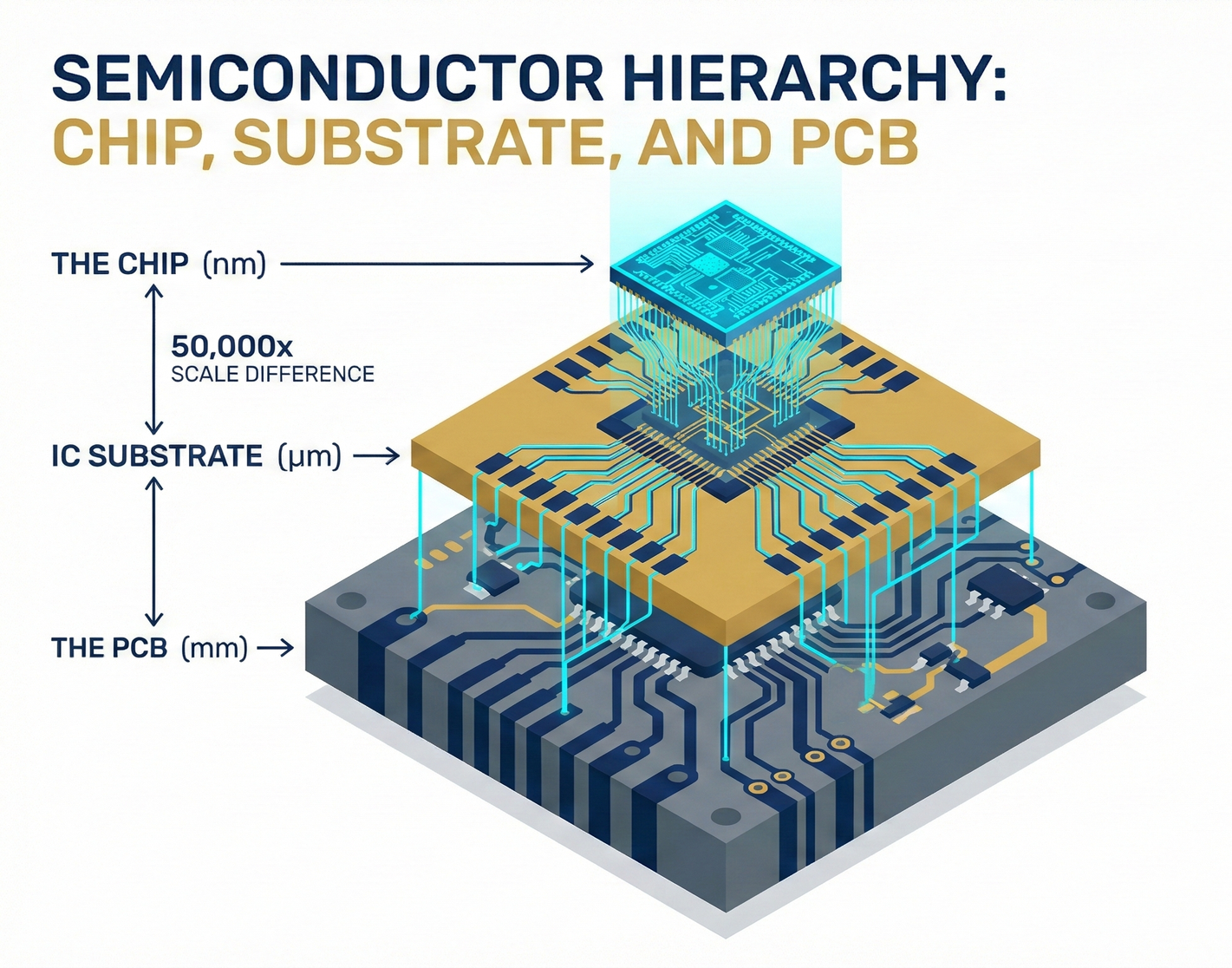
If you disassemble an AI server and look down through a microscope, you will see a three-dimensional world, much like a 'Russian nesting doll', composed of three completely different physical scales:
Layer One: Chip (Chip / IC / Die) — The Nanometer-Scale City Center
- Physical Scale: Nanometer (nm).
- This is the domain of TSMC and the 'brain' of the entire machine.
- The wires inside the chip are only 2 to 3 nanometers wide, tens of thousands of times thinner than a human hair. It is packed with tens of billions of transistors responsible for computation.
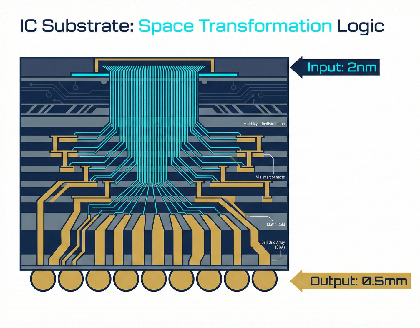
Layer Two: IC Substrate — The Micrometer-Scale Expensive Mattress (Adapter)
- Physical Scale: Micrometer (µm).
- Purpose: Space Transformation.
- Why can't the brain be placed directly on the bottom-most motherboard? Because there's a huge discrepancy in size. The circuitry on the chip is 2 nanometers, while the circuitry on the bottom-most motherboard is approximately 100 micrometers (equivalent to 100,000 nanometers). The difference in thickness between these two is an astonishing 50,000 times.
💡 Investor's Simple Analogy: Welding Spider Silk onto a Water Pipe
If you were to place a chip directly on a motherboard, it would be like asking a plumber to precisely weld a 'razor-thin strand of spider silk' onto a 'thick, bulky water pipe'. Physically, this connection is impossible.
Therefore, we need the IC substrate, this high-tech 'funnel' and 'mattress'.
It receives the dense, invisible nanometer-scale signals from the bottom of the chip, and then, within the substrate, gradually 'enlarges and widens' the spacing through layers of circuitry. By the time the signals reach the very bottom of the substrate, they have transformed into visible metal solder balls (approximately half a millimeter). At this point, they can be easily soldered onto the motherboard.
Layer Three: PCB (Printed Circuit Board) — The Millimeter-Scale Superhighway
- Physical Scale: Millimeter (mm).
- This is the 'main road' at the very bottom. When you open a computer case, the largest board you see, usually green or black, is the PCB (commonly known as the motherboard).
- It is the physical skeleton of the entire server. It is filled with IC substrates holding chips, power supplies, various cooling fans, and network interfaces. It is responsible for connecting all organs of the entire machine.
The Hidden Layer Zero: CCL (Copper Clad Laminate) — The Asphalt for Paving the Road
- In financial news, PCB and CCL often appear together, but they represent an upstream-downstream relationship.
- If the PCB is the constructed superhighway, then CCL is the 'raw asphalt material' used to pave this superhighway.
- PCB manufacturers (such as Gold Circuit Electronics and Tripod Technology) must first purchase this 'asphalt (copper clad laminate)' from CCL material suppliers (such as Taiwan Union Technology Corporation and ITEQ Corporation) before they can etch circuits, drill holes, and ultimately produce motherboards.
Strategic Convergence: This is a journey that becomes more grounded the further down we go.
By understanding this three-tiered, bottom-up and top-down (chip $\rightarrow$ substrate $\rightarrow$ PCB) hierarchical structure, we will not get lost in the hardware terminology that follows.
Our first stop is to delve into the 'micrometer-scale mattress' situated between the brain and the road, responsible for connecting the past and the future — the IC substrate.
Not only is the manufacturing process for this mattress extremely difficult, but what's even more absurd is that the core insulating material for this high-tech funnel, which controls the choke point of global AI computing power, has been monopolized for twenty years by a Japanese company that sells MSG.
In-depth Research · Quantitative Perspective
Want more semiconductor quantitative research insights?
【Insight Subscription Plan】Bid Farewell to Retail Investor Mentality: Build Your Alpha Trading System with 'Quantitative Capital Flows' and 'Consensus Data'EDGE Semiconductor Research
📍 Series Map — Navigate the Complete EDGE Semiconductor Research →


