In the previous chapter, we mentioned that IC substrates are like a "funnel," responsible for magnifying and converting nano-scale chip traces into micron-scale solder balls.
But have you ever wondered what the "walls" of this funnel are made of? Since dense copper traces need to be laid inside for conduction, the walls themselves must be an absolute insulator; otherwise, the entire substrate would short-circuit and burn out.
Before the 1990s, engineers typically used "liquid epoxy resin" as an insulating paint, applying it layer by layer. However, as computer CPUs became faster and traces became finer, a fatal flaw of liquid materials emerged: they dried too slowly and were applied unevenly. Even a slight ripple on the surface would cause the extremely fine copper traces laid on top to break.
Just as tech giants like Intel were scrambling for a solution, a savior appeared. And this savior, surprisingly, came from the kitchen.
🍜 Chapter 1: Ajinomoto's Unexpected Hegemony
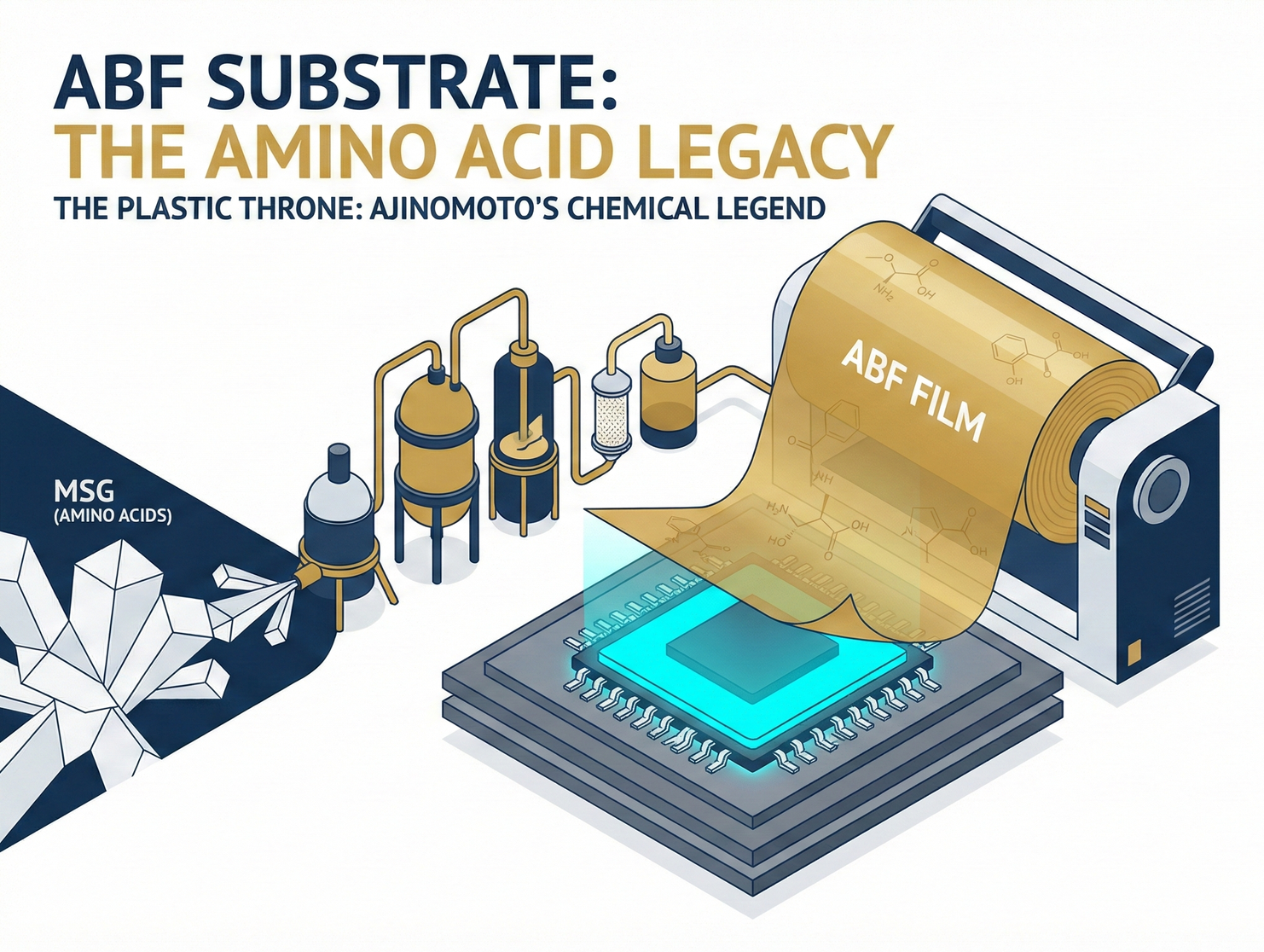
This is a long-standing yet incredibly true cross-industry legend in the semiconductor world. The century-old Japanese food giant Ajinomoto, known to us as the inventor of MSG, currently holds a terrifyingly high 99% market share in the global insulation material market for high-end computing substrates.
This accidental hegemony originated from an unintentional discovery in a chemical laboratory.
1. The Miracle of Amino Acid By-products
In the 1990s, Ajinomoto chemists were researching food amino acid by-products in their laboratories, attempting to find new chemical applications. They unexpectedly synthesized an extremely special "thermosetting resin."
The researcher, Shigeo Nakamura, keenly discovered that this chemical compound, originally completely unrelated to semiconductors, perfectly solved a critical pain point in the tech industry at the time. It possessed three revolutionary physical properties:
- Film Form: This was the greatest revolution! It could be made into "dry films" in rolls. Just like high-tech double-sided tape, wafer fabs no longer needed to painstakingly apply liquid and wait for it to dry. By simply peeling it off, laying it flat on the board, and applying heat and pressure, it would form a perfectly flat insulating layer.
- Excellent Insulation and Low Loss: Its molecular structure is extremely stable. When high-frequency, high-speed signals (such as current PCIe 5.0 or even 6.0) run around it, there is virtually no leakage or signal attenuation.
- Laser-friendly: Substrates have multiple layers, and holes (vias) must be drilled between layers to connect the copper traces. These holes are too small for traditional mechanical drills, requiring lasers to cut through them. ABF film has excellent absorption of laser energy; a single laser pulse instantly burns a perfectly smooth micro-via, without melting into a viscous blob of plastic.
2. Intel's Discernment and the Birth of a "Kingmaker"
No matter how good a material is, it needs someone daring enough to use it. In 1999, Intel, then the PC hegemon, was developing a new generation of processors and struggling to find a substrate material that could support extremely fine traces. When Intel engineers encountered Ajinomoto's invention, named ABF (Ajinomoto Build-up Film), they were utterly amazed.
Intel immediately signed a comprehensive cooperation agreement with Ajinomoto and fully integrated ABF substrates into its own processor packaging. This was a "kingmaker" moment. Once industry leader Intel gave its approval, the entire semiconductor supply chain followed suit. ABF thus became the sole industrial standard for high-performance computing (HPC) substrates worldwide.
3. An Irreplicable Chemical Moat
Over two decades have passed; haven't other major chemical companies (such as DuPont, Hitachi Chemical) tried to replicate this formula? The answer is: they have tried, but all have failed completely.
This is because ABF contains an extremely complex mixture of various chemical fillers and epoxy resin ratios. This constitutes a top-tier trade secret, accumulated by Ajinomoto based on its "century of food amino acid research," so much so that they disdain applying for patents (patent applications require public disclosure of the formula). This chemical moat is so deep that even American tech giants cannot cross it.
Strategic Status: As of 2026, whether it's NVIDIA's B200 / H100, priced at millions of New Taiwan Dollars, AMD's EPYC server processors, or the powerful Apple M series chips in your MacBook, their foundations are all firmly cushioned by this "MSG film" produced by Ajinomoto. As long as AI servers continue to ship, Ajinomoto's factories cannot stop for a moment.
How are ABF substrates manufactured?
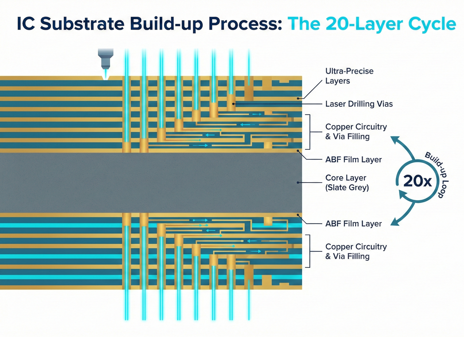
Remember a core concept: it is not "printed" like a printer; it "grows" layer by layer, like building a multi-story structure. In the industry, we call this the Build-up Process.
🏗️ Chapter 2: Building a Thousand-Layer Cake —— The Build-up Process
To construct this microscopic edifice supporting AI chips, engineers must follow an extremely intricate process with zero tolerance for error:
1. Core Layer —— The Rigid Foundational Framework
At the very center of this entire structure is a relatively rigid board (usually FR4 material reinforced with fiberglass). It provides physical support, ensuring the entire substrate remains firm. Large through-holes are first drilled into this foundation to enable electrical conduction between the upper and lower layers.
2. The Relentless Build-up Loop
Once the foundation is laid, the "thousand-layer cake" stacking steps are repeated continuously:
- Step 1: Lamination: Ajinomoto's dry ABF film is smoothly applied to both the upper and lower sides of the core layer and then cured and hardened using high temperature and pressure to form an insulating layer.
- Step 2: Laser Drilling: Advanced laser machines are used to precisely drill tens of thousands of tiny holes (vias) into the newly laminated ABF film.
- Step 3: Desmear: After the laser burns through the plastic, residual melted black residue remains in the holes. Strong chemical solutions, such as potassium permanganate, must be used to thoroughly clean the holes, leaving them spotless.
- Step 4: Plating: The entire board is submerged in an electroplating bath, allowing copper metal to fill the tens of thousands of micro-vias just drilled, and simultaneously forming ultra-fine conductive traces on the surface.
Repeat Cycle: Then, on the newly formed copper traces, another new layer of ABF film is applied, followed by laser drilling, cleaning, and copper plating... this process is repeated layer by layer, building upwards.
3. The Cruel Reality of the Layer Count War
- The substrates for ordinary PC or laptop CPUs, like those you and I use, typically require only about 8 to 10 layers.
- However, for top-tier AI chips like the NVIDIA B200, which must accommodate an enormous number of signal lines and a massive power delivery network, the substrate layer count skyrockets to 18 to 20 layers or even more!
- Manufacturing Difficulty: If, during the stacking of these 20 layers, even one layer gets a micron-sized dust particle, or the laser misses by 1 micron causing a copper trace to break, the entire "thousand-layer cake" that took several weeks to build will be directly scrapped. With each additional layer, the yield rate plummets "exponentially."
🦖 Chapter 3: The Curse of Large Area —— Why is the B200 Substrate So Difficult to Manufacture?
You may have seen in the news that TSMC's CoWoS advanced packaging capacity is extremely tight. However, the capacity for high-end ABF substrates is also on the brink of collapse.
The reason is simple: AI chips have become incredibly massive.
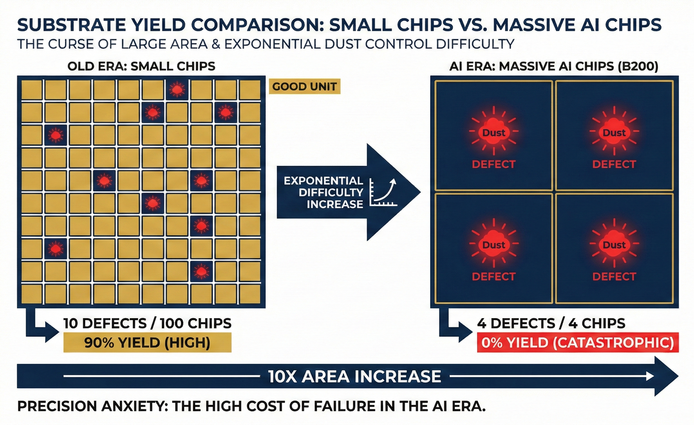
1. Relentless Increase in Size (Body Size)
In the past, the substrate size for a traditional CPU was approximately 30mm x 30mm (slightly larger than a postage stamp).
Now, NVIDIA's B200 architecture, by combining two massive GPUs and surrounding them with 8 High Bandwidth Memory (HBM) modules, results in the entire B200 substrate approaching a terrifying size of 100mm x 100mm!
This means that the area of a single substrate has surged by nearly 10 times or more.
2. The Despairing "Yield Math Problem" (Yield Math)
Substrate manufacturers produce these by placing large production panels into machines simultaneously.
- For small chips (30x30mm): A large panel can yield 100 small substrates. If 10 dust particles (defects) randomly fall during the process, at most 10 pieces are ruined, leaving 90 good ones. Yield rate is as high as 90%.
- For giant AI chips (100x100mm): From the same large production panel, because the B200 is so massive, only 4 large substrates can barely be cut from the entire panel. Here comes the challenge: If 10 dust particles randomly fall on this panel. If each of these 4 large substrates unluckily gets just one dust particle, all 4 pieces will be completely ruined, and the yield rate will directly become 0%!
This is why in the ABF substrate industry, "the larger the size, the harder the yield." This is also why only a handful of top-tier manufacturers worldwide have the ability to control micro-dust contamination and alignment precision in large-area processes, thereby building extremely high technological moats.
📊 4-1-1 Strategic Summary: The Warring States Era of the Three Major Substrate Manufacturers
The ABF substrate market is a brutal battlefield characterized by extremely high initial capital investment and high oligopoly. Only the following players stand at the apex of this plastic throne:
Conclusion:
- ABF is the most expensive "consumable": As long as TSMC ships an AI chip, a large and expensive ABF substrate will be consumed regardless. This is an absolutely essential market that grows with the explosion of computing power.
- The Cry of Physical Limits: Although Unimicron and Ibiden are striving to improve yield rates, plastic materials (ABF + fiberglass) have an inherent fatal flaw: warpage when heated. The enormous size of the B200, approaching 100x100mm, has pushed the warpage of plastic substrates to its physical limits. If the next generation of chips becomes even larger, plastic substrates simply won't be able to cope, and chips will detach directly from the board due to thermal expansion and contraction.
To solve this impending physical crisis, the semiconductor industry must completely abandon plastic foundations.
Next, we must utilize the oldest, yet also the flattest, material in human civilization——glass.
In-depth Research · Quantitative Perspective
Want more insights into semiconductor quantitative research?
【Insight Subscription Plan】Bid Farewell to Retail Investor Mindset: Build Your Alpha Trading System with 'Quantitative Capital Flows' and 'Consensus Data'EDGE Semiconductor Research
📍 Series Map — Navigate the Complete EDGE Semiconductor Research →


