Foreword: From Bent Wooden Boards to Absolutely Flat Steel Plates
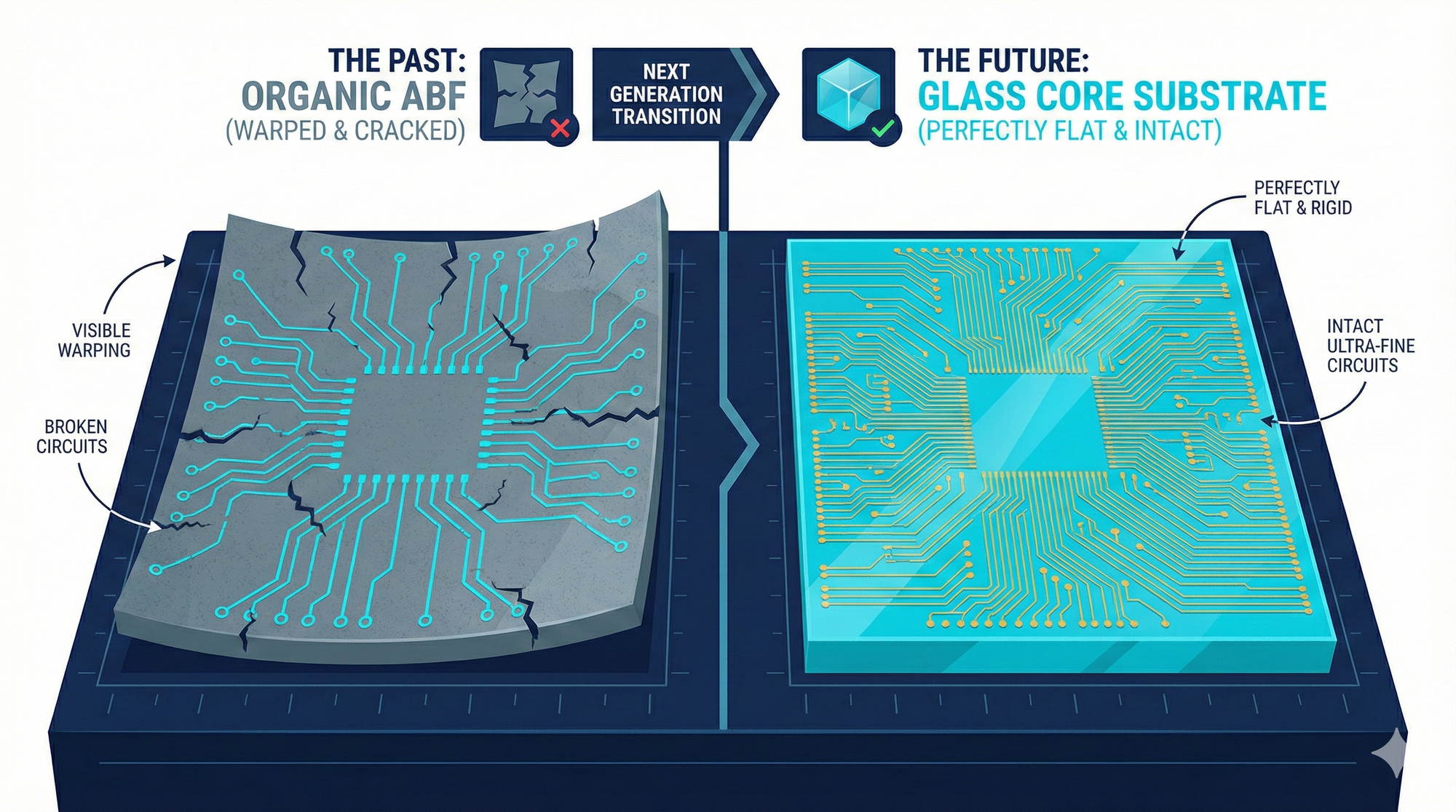
In the previous chapter, we saw that whether it's Japan's Ibiden or Taiwan's Unimicron, both face a daunting physical limit when manufacturing high-end ABF substrates: warpage.
As AI chips grow larger, the current NVIDIA B200 substrate size is approaching $100\text{ mm} \times 100\text{ mm}$.
You can imagine the current ABF plastic substrate as a "wooden board," and the chip as a 100-story skyscraper to be built on top. Wooden boards are inherently sensitive to heat and moisture. When this wooden board is sent into a reflow oven exceeding 200°C for high-temperature soldering, the board will inevitably undergo slight bending and undulations.
When only 10 stories are built, a slight bend in the wooden board can still be tolerated; but when we need to build 100 stories (stacking hundreds of billions of transistors and HBM memory) on it, even a single micron of bend in the foundation will instantly rupture the tiny circuits above, rendering the entire million-dollar AI chip useless.
To solve this critical flaw, semiconductor engineers arrived at a radical conclusion: we must remove the central wooden board and replace it with an absolutely rigid "steel plate."
In the microscopic realm of materials science, this steel plate is humanity's oldest invention—glass (Glass Core).
💎 Chapter 1: The Three Physical Superpowers of Glass Substrates
Please note that a glass substrate isn't an entire substrate made of glass, but rather the original ABF substrate's central supporting "core layer" is replaced with glass, while insulation layers and copper traces are still laid above and below.
But merely replacing this core layer delivers a "dimensional reduction strike" across three dimensions to existing ABF plastic substrates:
1. Ultimate Flatness: The Lithographer's Darling
- Pain Point: What semiconductor photolithography (lithography machines) fears most is an uneven surface. Because high-end lithography machines have an extremely shallow depth of focus, even a slight ripple on the substrate surface will blur the focus, preventing circuits from being printed.
- Glass's Superpower: The surface of glass achieves "atomic-level" absolute smoothness and flatness. This allows lithography machines to draw extremely fine lines on the substrate without obstruction.
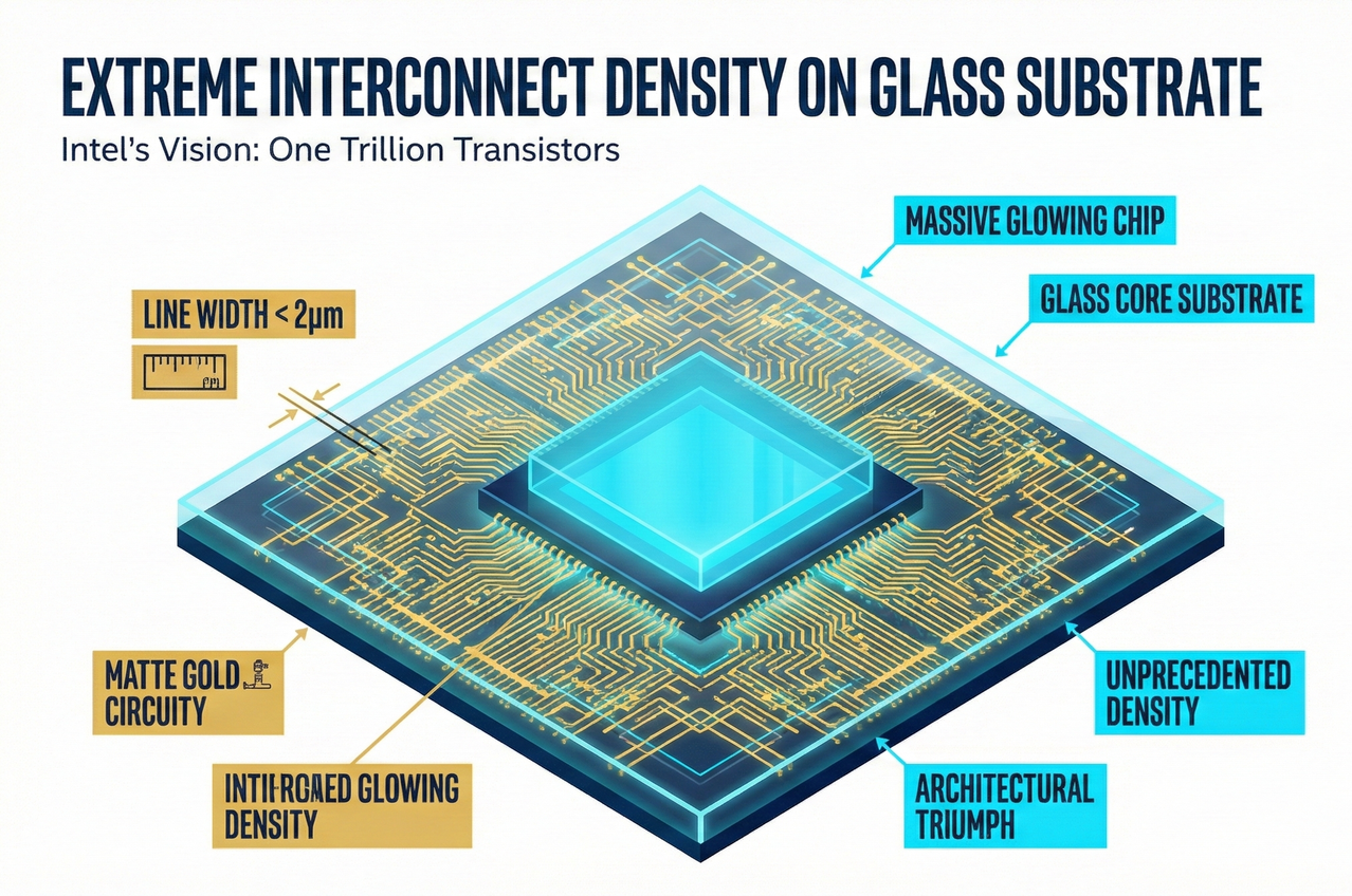
- Data Impact: The line width limit for traditional ABF substrates is typically stuck at around 5 microns; but glass substrates can easily support ultra-fine line widths less than 2 microns (< 2µm). This means the substrate's circuit density directly approaches "wafer-level" precision, allowing communication bandwidth between chips to multiply exponentially.
2. High Modulus: Completely Eliminating Warpage
- Pain Point: Plastic is too soft; large sizes inevitably bend.
- Glass's Superpower: Glass's Young's Modulus (a measure of material stiffness) is 3 to 4 times that of traditional ABF plastic. It is extremely rigid, remaining "rock-solid" even when baked at high temperatures above 200°C.
- Strategic Significance: This gives packaging manufacturers significant confidence. Because there's no warpage, engineers dare to make substrates extremely large (e.g., exceeding $200\text{ mm} \times 200\text{ mm}$), packaging 4 or even 8 giant GPUs on a single board at once. This is a realm plastic substrates can never achieve.
3. Thermal Stability: Breathing with the Chip
- What semiconductor packaging fears most is "uneven thermal expansion and contraction." There's a significant difference in the coefficient of thermal expansion (CTE) between silicon chips (the "brain") and ABF plastic (the "mattress"). When heated, plastic expands quickly while silicon chips expand slowly, creating strong shear stress between them that can tear solder joints apart.
- Glass's Superpower: The physical properties of glass are extremely similar to those of silicon chips; their CTEs are an almost perfect match! This means that when AI chips operate at full speed, generating intense heat up to 1000 watts, the glass foundation will "expand together with the chip at the same rate", perfectly offsetting destructive tensile forces.
⚡ Chapter 2: TGV (Through Glass Via) — Challenging the Paradoxical Limits of Materials Science
Since glass is so perfect, why haven't we used it sooner?
Because glass has a fatal flaw: it is too brittle.
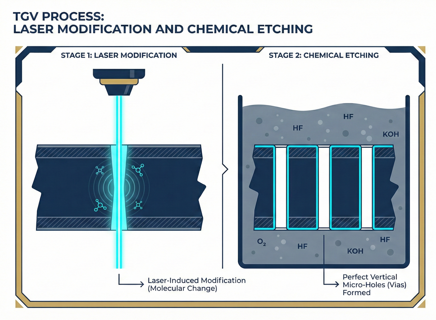
To allow electrical conduction between the top and bottom layers of the substrate, we must drill holes in the glass—hundreds of thousands of micron-sized holes, tens of times finer than a human hair. This technology is called TGV (Through Glass Via).
1. Traditional Mechanical Drilling? A Disaster Waiting to Shatter
On ABF substrates, we can use laser ablation or extremely fine mechanical drills (because plastic is elastic).
But what if you use a drill bit on a very thin piece of glass? Even a slight unevenness in stress will cause the entire sheet of glass to instantly shatter into a spiderweb-like waste, just like a broken car window.
2. The Ultimate Magic of TGV: LIDE (Laser Induced Deep Etching)
To resolve this paradox, equipment manufacturers invented a two-step magical process called LIDE (Laser Induced Deep Etching). This process perfectly combines optics and chemistry, making the drilling process incredibly elegant:
- Step 1: Laser ModificationEngineers do not aim to "burn through" the glass with a laser. They use extremely high-frequency ultrafast lasers (such as picosecond or femtosecond lasers) to instantly irradiate the interior of the glass. This laser beam does not destroy the glass, but rather precisely alters the "chemical molecular structure of the glass" along the laser's path, making this ultra-fine cylindrical trajectory particularly "vulnerable."
- Step 2: Chemical Wet EtchingNext, this seemingly untouched sheet of glass is immersed in a highly corrosive chemical solution (such as hydrofluoric acid, HF). Something magical happens: the solution specifically targets and etches away the "vulnerable" paths that were hit by the laser, at a rate 50 times faster than the surrounding normal glass!
- Result: Within minutes, hundreds of thousands of perfect micron-sized cylindrical holes, with extremely smooth inner walls and no cracks on the edges, are instantly formed in the glass. The glass body itself remains unharmed.
Equipment manufacturers capable of performing this drilling magic on brittle glass will become the most prominent "shovel sellers" in this glass revolution. Examples include German giant LPKF, and Taiwan's rare equipment dark horse with this capability—Tronco (8027.TW).
⚔️ Chapter 3: Who is Betting Big on Glass? — The Giants' Revenge and the Innovator's Dilemma
This is a future battle expected to see mass production officially kick off between late 2026 and 2027. In the current competitive landscape, there are three key players that cannot be ignored, each entering this battle with different ambitions and fears:
1. The Pioneer's Revenge: Intel's Killer Feature
If TSMC is the king of "wafer foundry," then Intel has always been a grandmaster of "advanced packaging."
- Strategic Motivation: Intel suffered significant losses in the wafer foundry battle at 7nm and below, but they view "glass substrates" as the ultimate trump card for a complete comeback after the 18A process.
- Trillion-Scale Ambition: Currently, NVIDIA's B200 chip incorporates over 200 billion transistors. Intel has boldly declared that, leveraging the extreme flatness and ultra-high density characteristics of glass substrates, they aim to achieve an astonishing 1 trillion transistors within a single chip package by 2030!
- Current Status: Intel has been quietly developing this for a decade in Arizona, USA, and has now established a highly scaled glass substrate pilot production line. This is not only for its own CPUs but also a secret weapon for Intel Foundry (its wafer fabrication division) to attract orders from cloud giants.
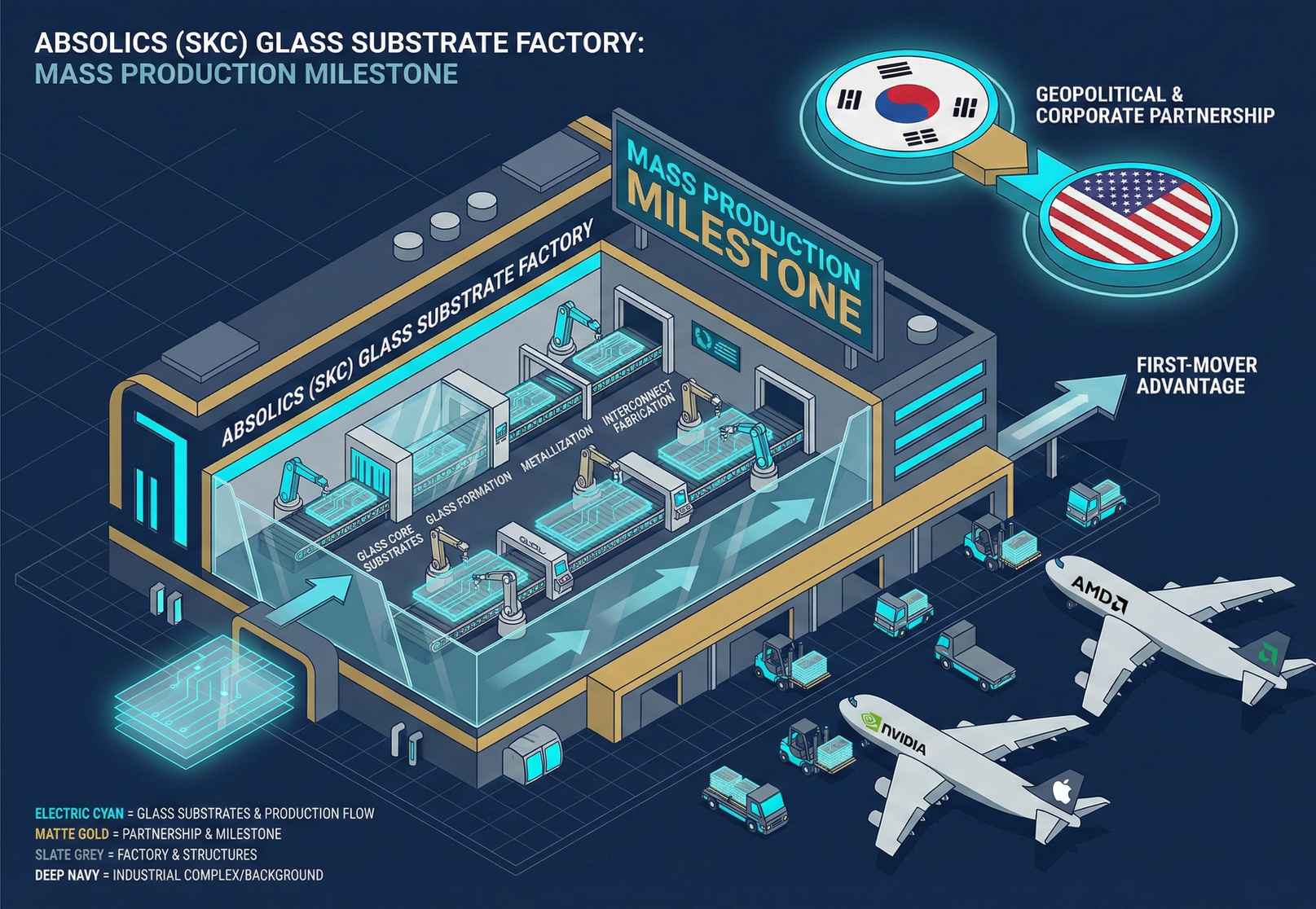
2. The Rushing Korean Dark Horse: Absolics' First Mass Production Plant
While Intel was still in pilot production, an unknown Korean company built a formidable facility in the U.S. and directly claimed the title of "world's first."
- Background: It is Absolics, a subsidiary of South Korea's SKC Group (specializing in chemical materials). They seized the vacuum period for glass substrates, investing heavily to build the world's first mass production factory "tailor-made for glass substrates" in Covington, Georgia, USA.
- Industry Impact: Due to the remarkably rapid progress of this factory, supply chain rumors suggest that AMD, NVIDIA, and even Apple, all grappling with TSMC's CoWoS capacity and the area limits of ABF substrates, are already queuing at Absolics' doors, eager to send their next-generation chips for testing. Koreans are attempting to seize the center of gravity for packaging substrate supply chains from Japan and Taiwan through glass substrates.
3. Taiwan's Dominant Player's "Innovator's Dilemma": Unimicron's (3037.TW) Defensive Counterattack
While the world is going crazy for glass, the most anxious is undoubtedly the current ABF plastic substrate leader—Taiwan's Unimicron.
- Conflicting Mindset: Unimicron faces the classic "Innovator's Dilemma." They have made significant profits from ABF substrates. If they fully embrace glass now, it would be akin to taking their own life, rendering newly acquired tens of billions of dollars worth of ABF equipment obsolete prematurely; but if they cling to plastic, they fear a direct dimensional reduction strike from Intel and Korean manufacturers three years later.
- Confidence and Actions: As an industry veteran, Unimicron has chosen the most stable "defensive counterattack." On the surface, they continue to increase ABF yield to generate cash, while discreetly forming alliances with international glass giants (such as Corning or Germany's Schott) and establishing a highly confidential glass substrate pilot production line internally. Once the trend for glass substrates is established in 2027, Unimicron, with its strongest customer relationships and deepest pockets, will undoubtedly be the substrate manufacturer in Taiwan most capable of instant transformation.
📊 4-1-3 Strategic Summary: The Ultimate Substrate Born for "Giant Chips"
This strategic summary table clearly contrasts the generational shift in materials science currently underway:
| Comparison Item | ABF Substrate (Organic Plastic Substrate) | Glass Substrate (Glass Core Substrate) |
|---|---|---|
| Core Material Property | Plastic (Softer, prone to warpage and deformation when heated) | Glass (Extremely rigid, absolutely flat, high temperature resistant) |
| Maximum Packaging Size | Approx. $100\text{ mm} \times 100\text{ mm}$ (B200 level) | Greater than $200\text{ mm} \times 200\text{ mm}$ (No upper limit) |
| Line Accuracy (Line Width) | > 5 microns (Limited by surface undulations) | < 2 microns (Approaching wafer fab's extreme precision) |
| Current Fatal Flaw | Yield rate plummets dramatically at large sizes | Fragile (Prone to breakage during production line handling and assembly) |
| Main Proponents | TSMC (CoWoS), Unimicron, Ibiden | Intel, Absolics (SKC), Samsung |
| Applicable Strategic Scenario | All GPUs / CPUs from now until 2026 | After 2027, super AI chips moving towards trillion-transistor counts |
💡 Capital Market Investment Keywords (The Winners):
- Exclusive "Shovel Seller" — Tronco (8027.TW): For glass substrates to achieve mass production, the most critical bottleneck is "drilling holes in glass (TGV)." Tronco is one of Taiwan's very few equipment manufacturers with a deep foundation in TGV ultrafast laser technology and has already gained certification from major American manufacturers (Intel). As soon as the capital market begins to hype glass substrate themes, its growth potential becomes immense.
- Transforming Giant — Unimicron (3037.TW): Although a dominant player of the old era, among substrate manufacturers in Taiwan, it is the most active and financially robust in preparing for glass. Investors should closely track its "capital expenditure (Capex)" flow over the next two years, as that will be the starting gun for mass production.
- Upstream Big Winner — Corning: Just like in the era of LCD panels, regardless of who downstream places the chips, the absolutely flat, impurity-free high-end glass substrate at the very source will ultimately have to be purchased from top-tier glass manufacturers like Corning. This is a unique business that is guaranteed to be profitable.
In-Depth Research · Quantitative Perspective
Want to gain more insights from semiconductor quantitative research?
【Insight Subscription Plan】Say Goodbye to Retail Investor Mentality: Build Your Alpha Trading System with "Quantitative Chips" and "Consensus Data"EDGE Semiconductor Research
📍 Series Map — Navigate the Complete EDGE Semiconductor Research →


