Introduction: The Secret in the Green Board —— From 'Burger Patty' to 'Premium A5 Wagyu'
Any electronic product we see in our daily lives contains a green Printed Circuit Board (PCB). You can imagine this PCB as a giant 'Big Mac burger,' which is formed by stacking and pressing layers of materials together.
In this burger, PCB manufacturers (such as Compeq and Chin-Poon Industrial) actually play the role of the 'chef'. The chef is responsible for cooking the patty, drilling holes, drawing circuits, and finally assembling the layers. However, the fundamental core that determines how good this burger tastes is the 'raw patty'.
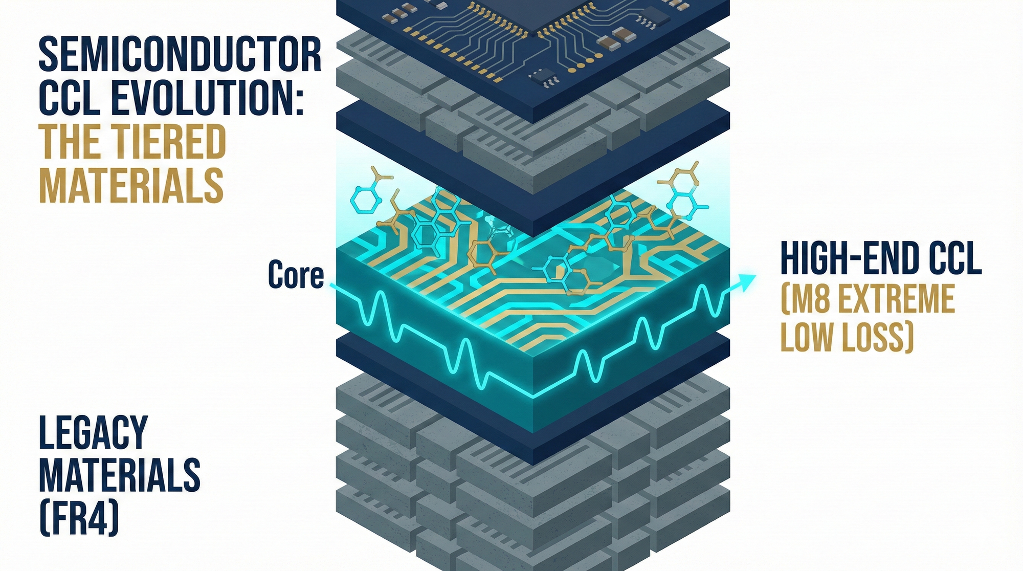
This raw patty is technically known in the semiconductor industry as CCL (Copper Clad Laminate).
CCL is a foundational material formed by pressing together 'insulating resin, supporting glass fiber cloth, and copper foil covering both sides'. In the era of traditional consumer electronics, everyone consumed affordable 'processed meat', and the chef's skill (the PCB manufacturer's process yield) determined success.
However, in the era of AI servers, the data transfer volume between chips is outrageously large (e.g., the formidable copper interconnect transmission within the NVIDIA GB200 NVL72 rack). If affordable processed meat continues to be used, the entire motherboard, under the bombardment of ultra-high-frequency signals, would directly become a useless board due to severe 'signal attenuation'.
In the AI era, if the meat quality (CCL material) does not reach the level of 'premium A5 Wagyu', even the best chef's skills are useless. Whether a piece of CCL is qualified to be used in AI servers is entirely determined by two cold, relentless physical parameters. Understanding these two parameters will give you a complete grasp of the underlying logic behind the soaring stock prices of high-end material manufacturers (such as TUC and ITEQ).
🧪 Chapter 1: The Crucible of Physics —— Dk and Df: The Arbiters of Computing Power
When signal frequencies reach AI server levels (such as PCIe Gen 5's 32Gbps, or even future PCIe Gen 6's 64Gbps and NVLink's 224Gbps PAM4 specifications), electronic signals are no longer merely water flowing obediently through copper wires but extremely sensitive 'electromagnetic waves'.
At this point, the insulating resin surrounding the copper wires (the core material of CCL) creates significant interference with electromagnetic waves. These two major interferences are Dk and Df.
1. Dk (Dielectric Constant) —— Dielectric Constant: Determining Signal 'Speed'
- Definition: This is an indicator of a material's ability to 'store electrical energy'. When electromagnetic waves pass through, the insulating material surreptitiously absorbs and stores a portion of the electric field energy, much like a small battery.
- Impact on signal (physical analogy): You can imagine Dk as the 'material of a running track'.
- High Dk materials (e.g., traditional FR4 epoxy resin): are like running on a 'soft, sandy beach'. Every step a signal (runner) takes, their foot sinks deep into the sand (electrical energy is absorbed and stored by the material), requiring greater effort to pull it out. The result is slow speed, severely dragging down performance, and causing significant 'signal latency'.
- Low Dk materials (e.g., high-end AI materials): are like running on an 'Olympic-standard PU track'. The surface is firm and provides excellent rebound, allowing a runner to spring forward instantly with each push.
- Physics Law: According to electromagnetic formulas, the propagation speed $v$ of an electromagnetic wave in a dielectric medium is inversely proportional to the square root of its dielectric constant $Dk$:$$v = \frac{c}{\sqrt{Dk}}$$(where c is the speed of light). Therefore, the lower the Dk value, the faster the signal travels. In AI cluster computing, which demands ultimate synchronization and extremely low latency, the Dk value is the critical baseline determining system response speed.
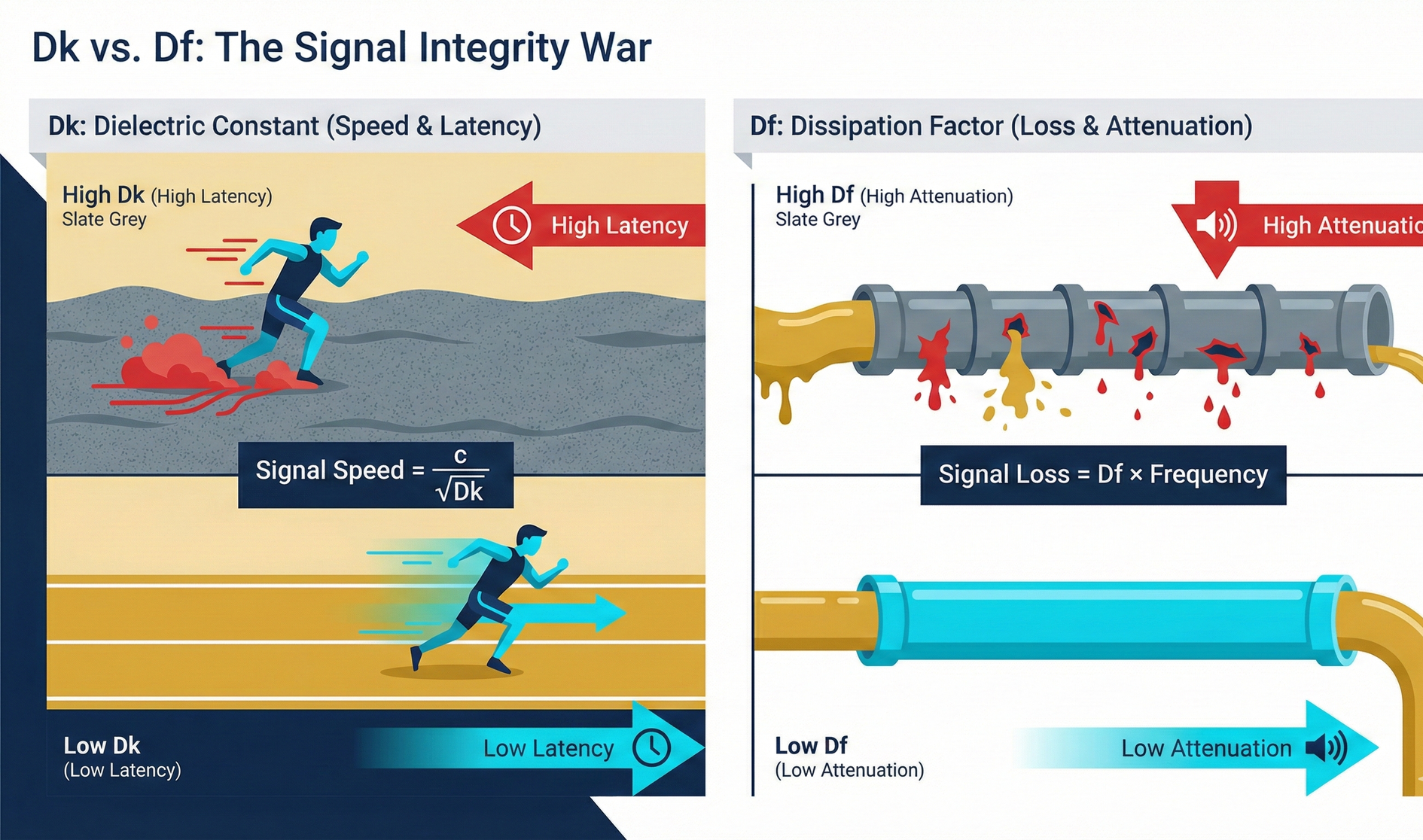
2. Df (Dissipation Factor) —— Dielectric Loss: Determining Signal 'Survival' 🌟
Dk only determines how fast a signal travels, but Df is the absolute key to determining whether a signal 'can survive to its destination'. This is also the ultimate indicator for which major CCL manufacturers are investing tens of billions in R&D and fiercely competing.
- Definition: This is an indicator of a material's ability to 'convert electrical energy into heat'. When ultra-high-frequency AC signals pass through, molecules within the insulating material frantically oscillate and reorient themselves with the electric field. This molecular friction, occurring tens of billions of times per second, generates enormous heat, wasting precious signal energy.
- Impact on signal (physical analogy): You can imagine Df as 'holes in a water pipe'.
- High Df materials: are like a water pipe with tiny holes everywhere. When the faucet (transmitting chip) is turned on full, sending water out with extreme pressure, water continuously leaks from the holes along the way (converted into heat). By the time it reaches the destination (receiving chip), the once torrential flow is reduced to mere drops.
- Low Df materials: are like a flawless titanium alloy pipe, where signals can be transmitted 100% completely from point A to point B.
- Why does AI fear it so much? The 'Curse of Exponential Magnification' In the past low-frequency era (low water pressure), a few holes in the pipe were insignificant. However, as we enter the ultra-high-frequency AI era of 112Gbps or even 224Gbps, high frequencies intensify molecular friction, and the signal loss caused by Df is 'exponentially magnified'. At the extreme frequency of 224Gbps, if the wrong material is used (a high-Df substrate), the originally clear digital signals '1s and 0s' will attenuate into unrecognizable noise (the Eye Diagram will completely close) in less than 5 centimeters of transmission on the motherboard. This is why NVIDIA's material requirements for server motherboards are so extreme: the Df value must approach zero infinitely.
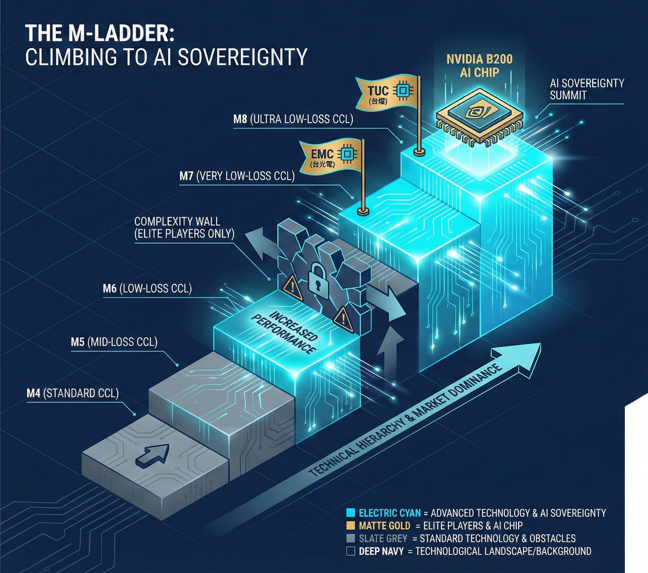
📈 Chapter 2: The M Ladder —— Six Legendary Tiers
To quantify these complex physical indicators, the semiconductor and PCB industries typically use the pioneering high-frequency material standard from Panasonic's Megtron series to classify CCL materials.
This is an 'M ladder' where the higher you go, the rarer the air and the more exorbitant the profits. Each decimal point decrease in Df value represents a decade of material scientists' dedication.
From this table, you can clearly see that when servers transition from traditional Intel platforms (M6) to NVIDIA's AI servers (M7/M8), the underlying materials undergo a qualitative transformation, akin to 'punching above their weight class'. Achieving this transformation relies not on purchasing more expensive equipment, but on a complete revolution in chemical formulations and metallurgical technology.
🔬 Chapter 3: The Dual Revolution of Chemistry and Metallurgy —— PPO Resin and HVLP Copper Foil
To forcibly reduce a board's Df value from 0.009 (M4) to below 0.002 (M8), CCL manufacturers must simultaneously wage two extreme microscopic battles: one in 'resin formulations' and another on 'copper foil surfaces'.
1. The Revolution in Resin Chemistry: From Epoxy Resin to PPO/PPE
Traditional CCL (such as M4 grade) uses epoxy resin. It is extremely inexpensive, easy to process, and has good adhesion, but it inherently possesses 'polarity'. Under the stress of ultra-high-frequency electric fields, these polar molecules intensely rub against each other, leading to extremely high Df loss.
To achieve the M7/M8 AI standard, CCL manufacturers must completely abandon epoxy resin and switch to an extremely expensive engineering plastic with a highly symmetrical and non-polar molecular structure: PPE (Polyphenylene Ether) or PPO (Polyphenylene Oxide).
- A5 Wagyu formulation secret: Introducing PPO is like upgrading a burger patty from processed meat to premium A5 Wagyu. PPO's electrical properties are perfect, allowing both Dk and Df to be minimized. However, it has a fatal flaw: it is extremely difficult to dissolve, extremely difficult to process, and 'does not adhere at all'!
- How to perfectly blend non-adhesive PPO resin, various flame retardants, and inorganic fillers together like a witch brewing a potion, and then bake it without bubbles or brittleness? This is the 'proprietary chemical formulation Trade Secret' that TUC and ITEQ keep locked in their safes, not even applying for patents. This chemical barrier remains insurmountable for Chinese CCL manufacturers to this day.
2. The Revolution in Metallurgical Physics: HVLP and the Skin Effect
With the insulating resin settled, the next challenge is the 'copper foil' used for conduction. In the world of ultra-high frequencies, electrons exhibit a peculiar physical behavior—the Skin Effect.
- What is the Skin Effect? When frequencies are extremely high, the magnetic field within the current forces electrons outwards, causing all current to flow not through the interior of the copper wire, but entirely on the outermost 'skin' of the copper wire. The higher the frequency, the thinner this skin (in AI servers, the current flow depth can be as little as 1 micrometer!).
- The 'Heaven's Road' Curse: Traditional copper foil, to 'grip' the resin tightly (to increase peel strength), is intentionally made very rough by copper foil manufacturers, like a microscopic mace. However, in the high-frequency era, this becomes a disaster. When all electrons are squeezed to flow on the surface, the rough surface is like the 'Heaven's Road' obstacle course climbed by special forces soldiers. Electrons crawling on the uneven, mace-like surface travel several times the actual distance, leading to significant resistance and signal loss.
- Solution: HVLP Copper Foil (Hyper Very Low Profile) To ensure smooth electron flow, the copper foil surface must be made 'absolutely smooth, like a mirror'. But this introduces a terrible contradiction: If the copper foil is as smooth as a mirror, and high-end PPO resin is 'naturally non-adhesive,' wouldn't the board simply fall apart when these two layers are pressed together?
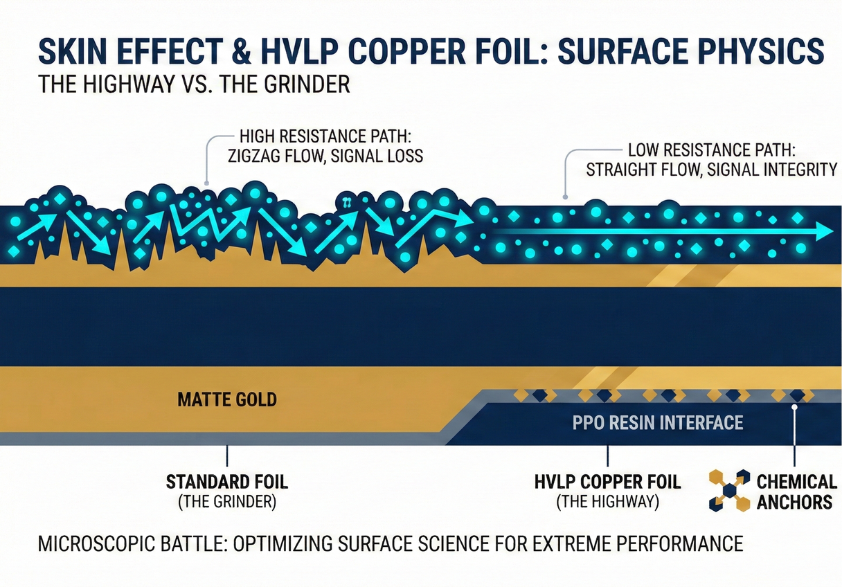
This is the ultimate technical barrier for high-end M8 substrates: How to utilize extremely specialized chemical coupling agents and surface treatment technologies to make 'extremely smooth HVLP copper foil' and 'completely non-adhesive PPO resin' bond tightly together, so that the board does not 'delaminate' even after going through a 260°C high-temperature reflow oven?
Whoever can perfectly resolve this 'contradiction of physics and chemistry' will secure NVIDIA's exclusive orders.
(註:This has also elevated the strategic position of high-end HVLP copper foil manufacturers in Taiwan, such as Gintech (8358.TW).)
📊 4-2-1 Strategic Summary: Materials, The Source of All Profit
For your reference, we summarize this fundamental physics battle in a straightforward strategic table:
Elevation in Business Thinking:
Through this in-depth physical and chemical analysis, we arrive at an extremely important investment logic: in the AI server hardware supply chain, the 'moat' of the 'materials segment' is far deeper than that of the 'manufacturing segment'.
PCB manufacturers can learn to drill holes by purchasing expensive laser drilling machines; but the PPO blending ratio and chemical cross-linking agent formulation that CCL manufacturers keep locked in their safes are 'Black Magic' that Chinese manufacturers cannot replicate even by poaching engineers and spending three to five years trying.
In-depth Research · Quantitative Perspective
Want more semiconductor quantitative research insights?
【Insight Subscription Plan】Bid Farewell to Retail Investor Mentality: Build Your Alpha Trading System with 'Quantitative Chips' and 'Consensus Data'EDGE Semiconductor Research
📍 Series Map — Navigate the Complete EDGE Semiconductor Research →


