After we completed the construction of the "superhighways" (PCBs and CCLs) inside AI server chassis, we now face an even greater challenge: how to enable this immense computing power to extend beyond the chassis and connect thousands of GPUs to form "compute clusters"?
In the world of data centers, connecting two servers is not arbitrary but rather depends on an extremely crucial variable: "distance". This represents a hierarchical system between electronic and photonic transmission, and on the threshold of the 1.6T era, this system is undergoing a destructive reshaping.
🛑 Chapter 1: The Punishment of Distance — The "Hierarchical System" of Data Center Transmission
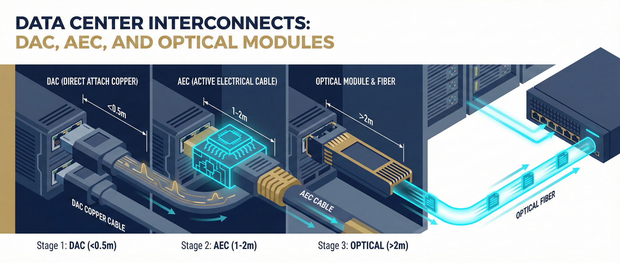
In AI cluster architectures, signal transmission adheres to a strict "physical lifeline":
- < 1 meter (within the rack): DAC (Direct Attach Copper) This is a passive copper cable, simple in structure, unpowered, and the cheapest option. It serves as the "local street" within the data center. However, in the 1.6T era (single-lane 224Gbps), the effective transmission distance of DAC has been compressed to within 0.5 meters, meaning it cannot even span half a standard rack.
- 1 ~ 2 meters: AEC (Active Electrical Cable) By embedding Retimer chips at both ends of the cable, power is forcibly used to repair attenuated signals, barely allowing the copper cable to function for an extra 1 meter without turning into a "signal swamp."
- > 2 meters (across racks): Optical modules (AOC / Transceiver) When the distance exceeds 2 meters, the loss in copper cables becomes unreasonable. At this point, electrons must "transfer to an airplane," converting the signal into photons, and entering the world of fiber optic transmission.
Current Strategic Situation: As OAM (Compute Accelerator Module) and UBB (Universal Baseboard) standards adopted by AI servers become increasingly prevalent, the PCB content within AI servers has reached 5 to 7 times that of traditional servers. When this computing power needs to be interconnected, over 90% of connection distances exceed 2 meters. This implies that: expensive "optical transceiver modules" are required at both ends of every computing power superhighway.
🧪 Chapter 2: The Verdict of the Skin Effect — Why Copper Cables Fail in the 224G Era?
Why can't we simply make signals travel further by "thickening copper wires" or "increasing voltage"? This involves a critical phenomenon in high-frequency physics: the Skin Effect.
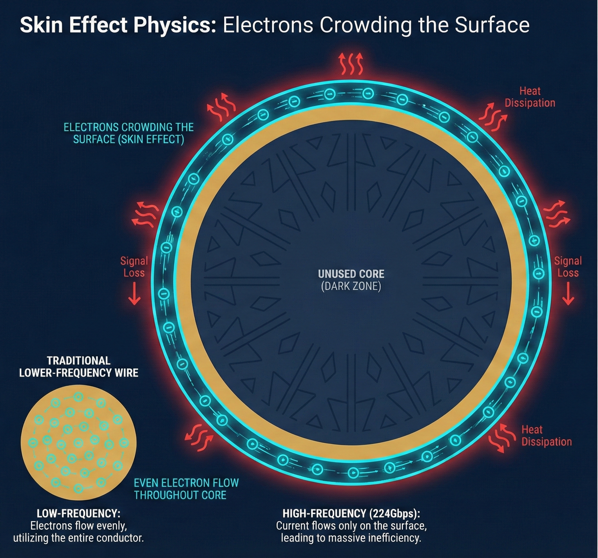
As the frequency of electrical signals increases (the standard frequency in the 1.6T era), electrons exhibit a peculiar "surface tendency." They no longer distribute uniformly throughout the copper conductor but instead crowd into the extremely thin "surface layer" of the wire. This leads to the following three devastating consequences:
- Dramatic Reduction in Effective Cross-sectional Area: Even if a copper wire is as thick as a thumb, the actual "channel" through which electrons can flow is reduced to a nanoscale thickness.
- Exponential Increase in Resistance: When frequency doubles, effective resistance does not increase linearly but rather jumps exponentially. At a single-lane bandwidth of 224Gbps, the signal attenuation rate of copper cable is so rapid that after traveling 0.5 meters, the signal transforms from a "high-definition digital waveform" into an unrecognizable "noise sludge."
- Transformation into a Heating Element: Due to the sharp increase in resistance, a large amount of signal energy is directly converted into heat during transmission. At this point, the copper cable is no longer a "data channel" but a "heating element." In AI racks where cooling space is extremely precious, this is an intolerable disaster.
📉 Chapter 3: Copper Retreats, Optics Advance — The Only Way Forward for Compute Clusters
Facing this physical barrier, global cloud service providers (CSPs) and major server manufacturers are compelled to shift resources from traditional copper cables to ultra-high-layer PCBs and advanced optics. This is not merely a technological evolution but a recalculation of "power consumption and cost":
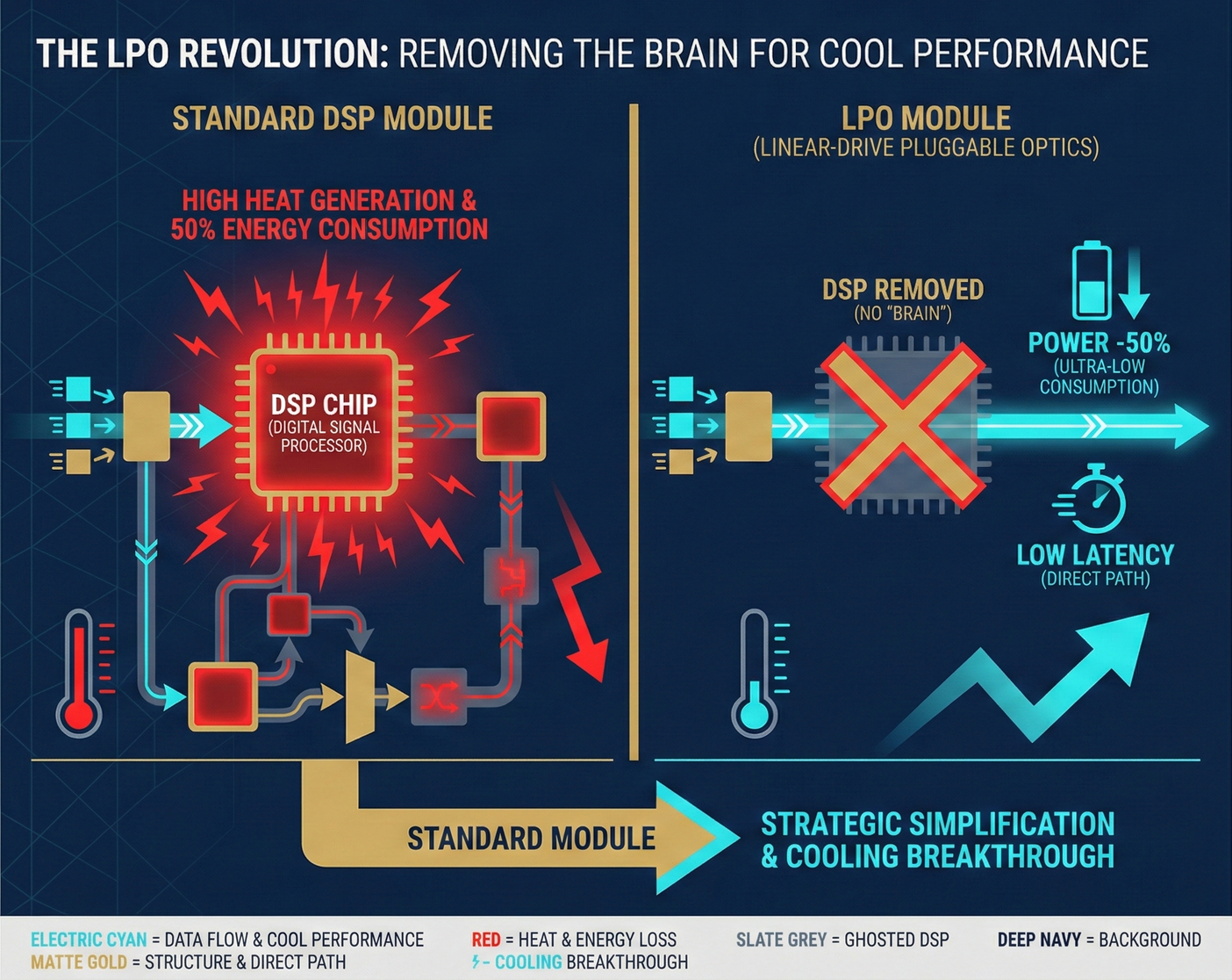
- Heat is the Biggest Enemy: 800G optical modules already make server front panels intolerably hot. At 1.6T, if the traditional architecture is maintained, optical modules plugged into the front panel would generate so much heat as to cause physical melting damage to the server.
- LPO (Linear Pluggable Optics) Strategic Maneuver: To address the power consumption challenge, the industry preemptively introduced a bridging technology called LPO before the ultimate CPO (Co-Packaged Optics). Its core logic is very aggressive: directly removing the most power-hungry DSP (Digital Signal Processor) chip inside the optical module.
- 50% Power Savings: Through this "brain removal surgery," LPO modules can save nearly half the power and significantly reduce transmission latency.
- 2026 Transitional Bonus: For many data center customers unwilling to wait for CPO standards to mature, LPO is a lifeline in the inaugural year of 1.6T.
- Trade-off: The responsibility for signal compensation is offloaded to the switch chip, which places higher demands on switch performance.
Conclusion: In the high-frequency era of AI, electrons can only travel within the "streets (PCBs)" inside the chassis. Once they need to travel longer distances, they must convert to photons. This market is undergoing a dual transformation in "volume" and "price"—the number of AI ASIC chips is expected to grow by over 65% year-on-year in 2026, driving demand for optical transceiver modules to more than 10 times that of traditional servers, with individual unit values soaring from hundreds to thousands of US dollars.
🚦 Chapter 4: Optical Transceiver Modules — The "Mouth" and "Ears" of Servers
If you walk into any hyperscale data center comprising tens of thousands of GPUs in 2026, you will see a row of fully plugged-in devices resembling oversized USB flash drives at the back of the servers—those are optical transceiver modules.
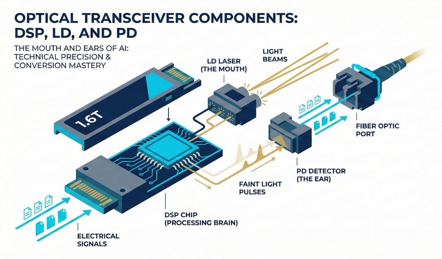
This is a sophisticated black box responsible for performing the most critical operations in AI computing: converting electrical signals into optical signals for transmission (E-to-O), and converting received optical signals back into electrical signals (O-to-E). It consists of three core internal components:
- DSP (Digital Signal Processor) — The Brain: This is the most expensive electronic chip in the entire module, responsible for repairing and aligning dirty and attenuated signals during transmission, ensuring that 1.6T data can be accurately read.
- LD (Laser Diode) — The Mouth: The core light-emitting component. In the 1.6T era, LDs must complete hundreds of billions of on/off cycles (or modulations) in an extremely short time, and the light purity must be exceptionally high.
- PD (Photodetector) — The Ears: Responsible for capturing faint light pulses from kilometers away (or several meters away) and converting them back into raw electrical signals.
Why is it so expensive that it's a headache for CSP giants?
A single 800G optical module costs approximately $1000~$2000 USD. Imagine a switch with 32 ports; the cost of simply populating it with modules often already exceeds the price of the switch itself.
🧠 Chapter 5: DSP — The "Brain Power" Monopolized by Two Giants
In the world of optical communications, there is a brutal supply chain rule: no matter how many manufacturers produce optical modules, if they cannot obtain DSP chips, not a single module can be shipped. This market is the absolute domain of American tech giants:
- Key Players: The global DSP market is primarily monopolized by two major powerhouses: Marvell (US) and Broadcom (US).
- Technological Bottleneck: Upon entering the 224G era, signal "nonlinear distortion" is extremely severe. Without DSPs performing powerful PAM4 modulation and compensation, optical signals would only be a mass of ineffective noise.
- Industry Standing: DSPs account for 20~30% of the cost of optical modules. For module manufacturers, Marvell and Broadcom are not just suppliers, but also the "chokepoint" that determines whether they can mass-produce 1.6T products.
⚔️ Chapter 6: The Battle of Optical Engines — EML vs. Silicon Photonics (SiPh)
This is a debate about the path forward concerning "materials science" and "economics": What material should we use to generate light?
- EML (Electro-absorption Modulated Laser) — The Traditional Noble:
- Material: Employs Indium Phosphide (InP) compound semiconductors.
- Status: This is currently the mainstream solution within the NVIDIA ecosystem. It offers pure light quality and mature technology, but its production cost is extremely high, and it is difficult to integrate with silicon wafer processes.
- SiPh (Silicon Photonics) — The Commoner's Revolution:
- Material: Primarily uses inexpensive Silicon (Si) wafers.
- Logic: Although silicon itself does not emit light, we can etch optical channels (waveguides) onto silicon chips and then attach an external laser source.
- Advantages: Can be mass-produced using TSMC's mature CMOS processes. As transmission rates enter 1.6T or even higher, Silicon Photonics' cost advantage and high integration will become a powerful disruptor.
📊 4-3-1 Strategic Summary: The Module's Distance Lifeline
Conclusion:
- The Golden Decade of Optical Modules: AI servers demand 5-10 times more optical modules than traditional servers, making this a highly profitable business characterized by both increased volume and price.
- Heat Dissipation is the Arch-Nemesis: By the 1.6T generation, we must consider "detaching" optical modules from the front panel and moving them next to the CPU. This is the CPO revolution we will explore in 4-3-4.
In-depth Research · Quantitative Perspective
Want to gain more semiconductor quantitative research insights?
【Insight Subscription Plan】Break Free from Retail Investor Mentality: Build Your Alpha Trading System with "Quantitative Chips" and "Consensus Data"EDGE Semiconductor Research
📍 Series Map — Navigate the Complete EDGE Semiconductor Research →


