In previous chapters, we discussed how optical modules serve as the 'mouth' of servers. However, as AI computing enters the 1.6T and even 3.2T era, the challenge we face is no longer 'how to transmit data,' but rather the spatial constraint of 'whether the organs can fit.'
The ultimate goal of this revolution is to transform data centers into a gigantic chip.
🛑 Chapter One: The End of Distance — Why "Proximity" is the Only Way Forward for AI Compute Power?
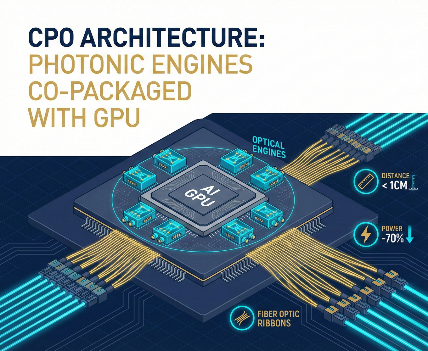
In the era of traditional pluggable modules, optical modules were placed on the front panel of switches, with a PCB trace distance of about 20 to 30 centimeters from the core switching chip (ASIC).
- The Power Consumption Black Hole: To drive electrons across 30 centimeters of copper wire without data loss, we must add powerful DSP chips for signal restoration. This leads to an absurd phenomenon: in the 1.6T era, the total power consumption of optical modules will account for over 50% of the switch's energy consumption.
- The Core Logic of CPO: The core logic of CPO (Co-Packaged Optics) is simply one word: "Proximity." We "attach" the optical engine directly onto the ASIC or GPU's substrate, shortening the distance to less than 1 centimeter.
- Power Salvation: Transmission power consumption can plummet from 15~20 pJ (picojoules) per bit to below 5 pJ, an energy efficiency increase of up to 70%. This is not just about saving power but also about preventing AI clusters from melting down due to overheating.
🏗️ Chapter Two: From NPO to CPO — Transitional Technical Compromises and Strategic Pathways
Technological revolutions are never achieved overnight. Before entering the ultimate 'electro-optical fusion,' the industry has a strategic intermediate transition solution: NPO (Near Package Optics).
- NPO (Near Package Optics): The optical engine is placed on the PCB, adjacent to the ASIC, but both are still on different substrates. This is relatively friendly for heat dissipation and maintenance and is a solution that Broadcom is currently strongly promoting and has already commercialized (such as the predecessor to the Bailly platform).
- Ultimate CPO: This is true "co-habitation" of optics and electronics. The silicon photonic chip (PIC) and electronic integrated circuit (EIC) are packaged together with the GPU onto the same substrate using 2.5D or 3D packaging. This is the ultimate vision for 2027, jointly defined by TSMC, Google, and Meta.
🔥 Chapter Three: "Optical-Electrical Separation" — The Heat-Sensitive Laser and the Business Opportunity of ELS (External Laser Source)
This is a cruel paradox in physics: silicon photonic chips require strong light, but the lasers that emit light are extremely sensitive to heat.
- Laser "Thermal Failure": Under high computational loads, GPU core temperatures often exceed 90°C. However, core laser components (such as InP lasers produced by Lumentum) operate optimally below 50°C. If lasers are packaged together with GPUs, their lifespan would shorten from several years to just weeks, which would be an absolute disaster in cloud data centers.
- ELS (External Laser Source) — The Wisdom of Split-System Air Conditioning: To resolve this contradiction, the industry developed the ELS (also known as RLS, Remote Laser Source) architecture.
- External Compressor Unit: The "heat source" laser source is moved out of the high-heat area and made into an independent box that plugs into a panel at the cold air inlet.
- The Value of Polarization-Maintaining Fiber (PM Fiber): Specialized PM fiber is used to transmit the "cooled" pure light source into the optical engine within the chassis.
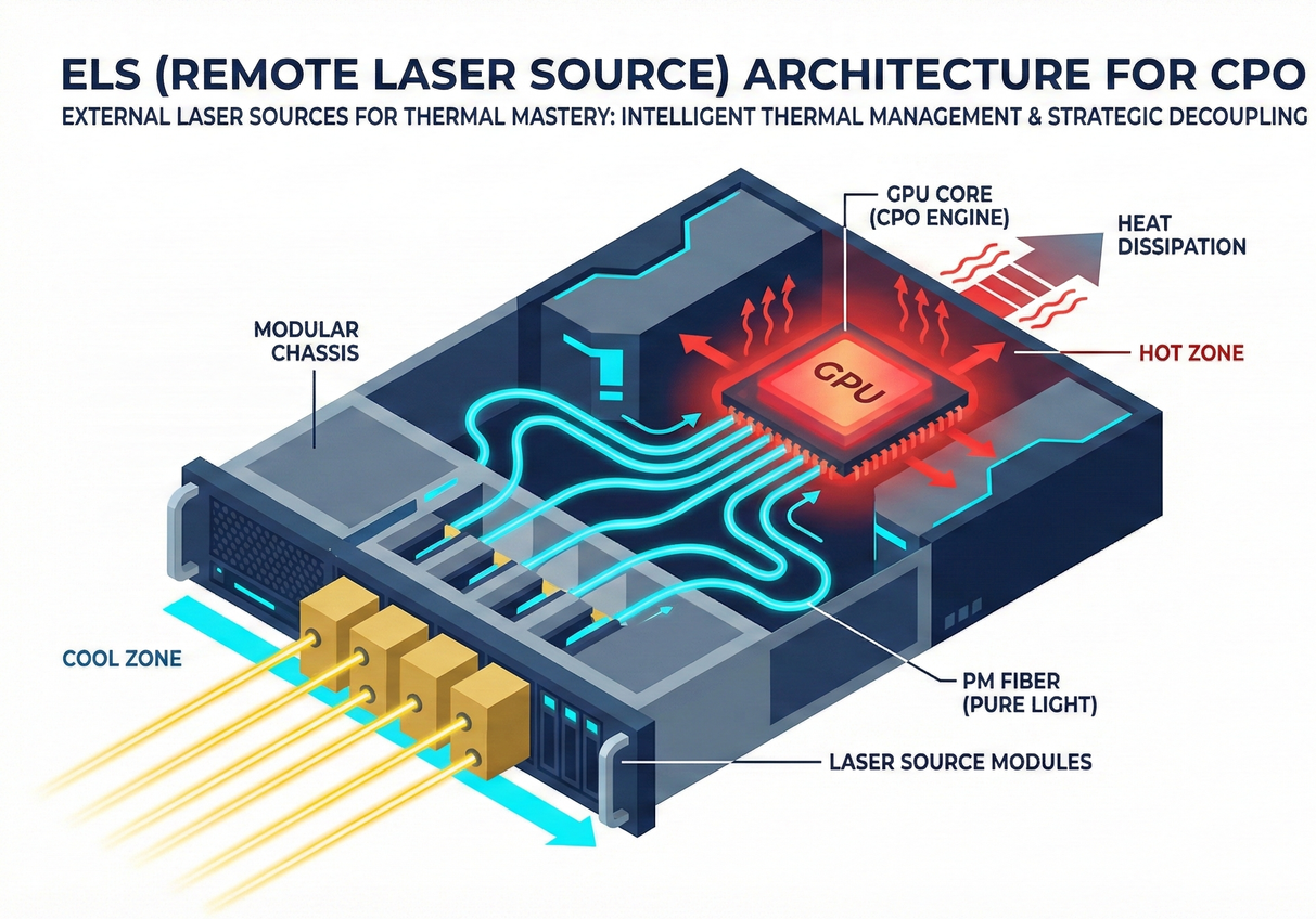
- Strategic Business Implications: This creates an entirely new market for "strategic resources." Manufacturers capable of providing high-power, low-loss, external laser sources (such as Lumentum, Optilink, and Wavelength Opto-Electronic), will, upon CPO's widespread adoption, gain control over the "gateway of light" and its associated revenue.
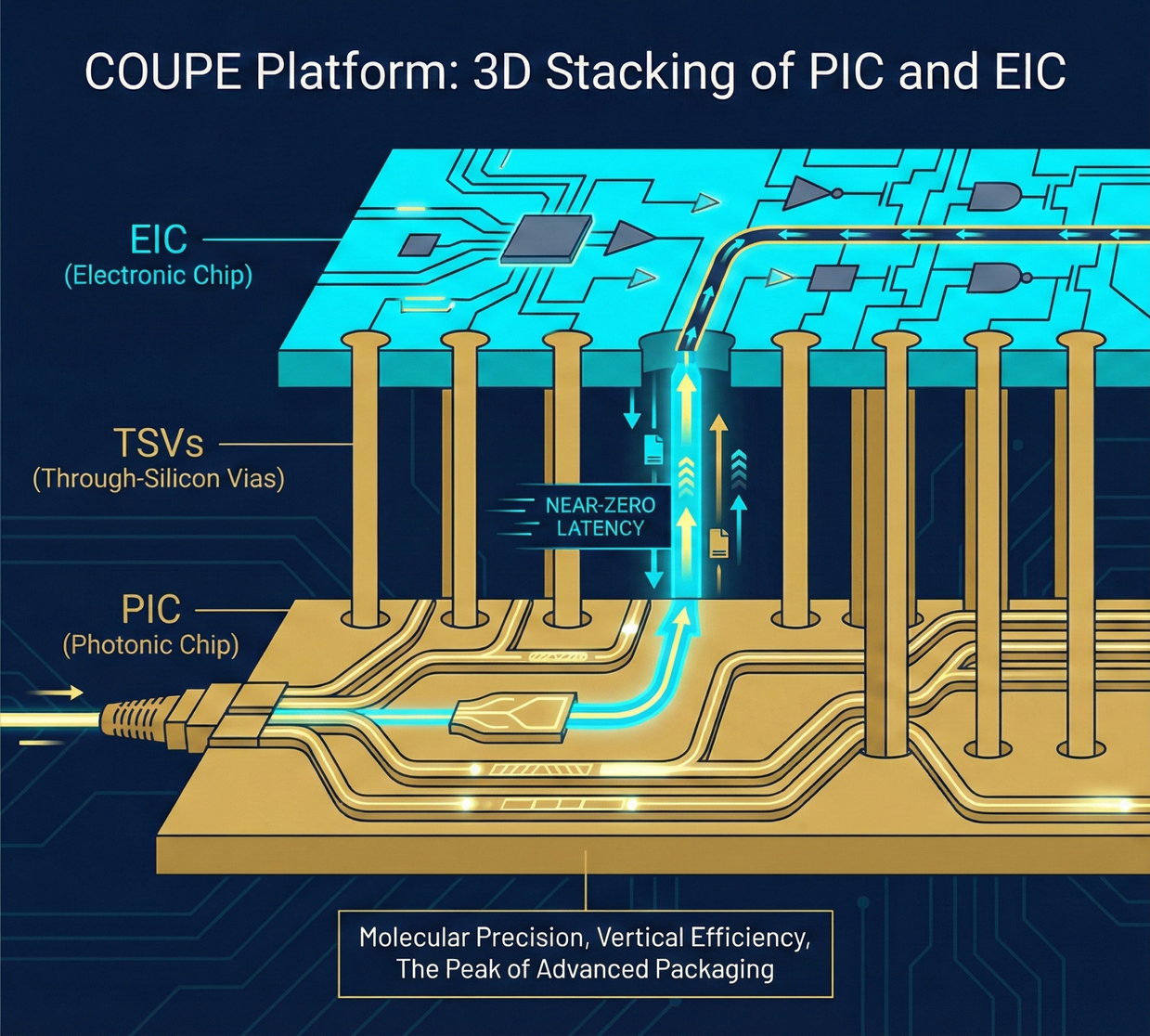
🏗️ Chapter Four: TSMC's Ultimate Black Technology — The COUPE Platform
TSMC's trump card in the CPO domain is called COUPE (Compact Universal Photonic Engine). This technology is expected to enter mass production between late 2025 and 2026, and it will fundamentally transform the efficiency limits of "electrical-to-optical signal conversion."
1. The Ultimate in 3D Stacking: SoIC-X Technology
In traditional silicon photonics modules, the PIC (Photonic Integrated Circuit) and EIC (Electronic Integrated Circuit) are typically laid out side-by-side on a substrate (2D or 2.5D layout). While this approach is mature, the wire lengths are still too long, leading to unnecessary impedance and power consumption.
- COUPE's Vertical Stitching: TSMC utilizes its SoIC (System-on-Integrated-Chips) packaging technology to directly "stack" the EIC on top of the PIC (3D Stacking).
- Zero-Distance Transmission: Through-Silicon Via (TSV) technology shortens the electro-optical conversion distance to the micron level. This reduces power consumption during signal conversion to its physical minimum while maximizing substrate space savings.
2. TSMC's "Full-Course Meal" Strategy
This is a key point you mentioned in the draft. TSMC is building a closed ecosystem that competitors cannot catch up with:
- Front-end: Providing you with the world's most powerful 2nm / A16 compute chips.
- Mid-end: Using CoWoS to package HBM memory for you.
- Back-end: Directly packaging the COUPE optical engine into the same system.
- Strategic Significance: When TSMC can offer a "one-stop" compute + transmission solution, clients (such as NVIDIA, Broadcom) will no longer need to seek external module manufacturers for complex secondary packaging. TSMC not only fabs the chips but also the "entire data highway."
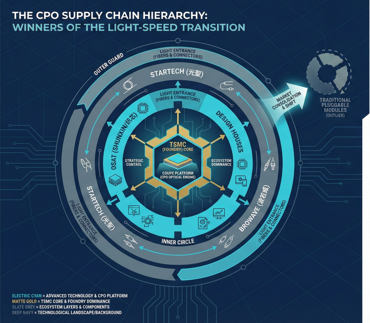
⚔️ Chapter Five: The Power Reshuffle of the Industrial Chain — Who are the Winners? Who is Being Marginalized?
The CPO revolution is not a gentle technological upgrade; it is a "resource grab" within the supply chain.
1. The "Marginalization" Crisis for Traditional Optical Module Manufacturers
In the past, optical module manufacturers (such as InnoLight and Coherent) were responsible for purchasing components from chip makers and assembling them into small black boxes. However, in the CPO era, that "shell" is gone, and the core silicon photonic chip is packaged by TSMC directly into the GPU.
- Value Dilution: If module manufacturers cannot transform to provide CPO optical engine design or ELS (external laser) systems, they will be relegated from "system suppliers" to "low-margin assembly service providers." This is precisely why many industry giants are frantically investing in silicon photonics design R&D today.
2. A New Blue Ocean for Taiwanese OSATs: Foxlink-KY (6451)
CPO requires extremely high-precision optical alignment packaging. While TSMC is strong, it focuses on the most critical 3D stacking, leaving a substantial amount of back-end optical sub-assembly (OE) and testing work to be supported by specialized OSATs.
- Foxlink-KY (6451): As Foxconn Technology Group's optical communications flagship, its accumulated expertise in SiP (System-in-Package) makes it one of the most competitive back-end OSAT partners in TSMC's COUPE ecosystem.
3. Connectors and Optical Path Components: Avantgarde (3363), Optilink, Wavelength Opto-Electronic
When optical fibers must be plugged directly into the chip core, special 'optical pathways' are required.
- Polarization-Maintaining Fiber and V-Groove: Avantgarde (3363) has collaborated with TSMC in silicon photonics for many years, and its specialized "polarization-maintaining fiber" alignment technology is a physical prerequisite for ELS systems. Optilink and Wavelength Opto-Electronic, in turn, have secured the last remaining physical domain in the CPO era that "cannot be replaced by wafer foundries" for external optical paths and connectors.
📊 4-3-5 Strategic Summary: The "Ultimate Destination" of Compute Power and Optics
Let's integrate this winner's map of the CPO revolution:
- Foundry - Absolute Big Winner 👑: TSMC, through COUPE, has seized ultimate power in silicon photonics manufacturing and 3D packaging.
- OSAT (Advanced Packaging and Testing) - Greatly Increased Opportunities: Companies with optical packaging experience, such as Foxlink-KY, will share in the substantial back-end optoelectronic testing orders.
- Connector/Fiber Optic Components - Invisible Champions 🚀: Avantgarde, Optilink, Wavelength Opto-Electronic. Because the act of "fiber optics needing to connect directly into the chip" cannot be digitized, the moat of precision mechanical processing remains robust.
- Traditional Module Manufacturers - Critical Transition Period ⚠️: Facing the threat of "de-boxification," they must transition towards ELS or CPO contract manufacturing.
Conclusion: While CPO is still on the eve of its explosion in 2026, TSMC's COUPE has already laid out the blueprint for its advance. This is no longer a border war between optical communications and semiconductors, but a new era of "optoelectronic semiconductors" where the two merge into one.
Deep Research · Quantitative Perspective
Want to gain more semiconductor quantitative research insights?
【Insight Subscription Plan】Break Free from Retail Investor Thinking: Build Your Alpha Trading System with "Quantitative Chips" and "Consensus Data"EDGE Semiconductor Research
📍 Series Map — Navigate the Complete EDGE Semiconductor Research →


