Positioning: This section first brings "packaging" back to physical reality to establish a global perspective; later, we will delve into advanced packaging terms such as CoWoS, HBM, and Chiplet.
<
Chapter 1: Overall Perspective: What is Packaging? — The End of the Semiconductor Journey and the "Embodiment of the Physical"
Before we dive into CoWoS, HBM, and Chiplet – these enticing terms that the global capital market is frantically pursuing – we must ask our readers to set aside all financial reports and revisit a fundamental physical common sense, one often overlooked by foreign analysts:
Consider this: If today you were to take a newly-produced, expensive 3nm AI chip directly from TSMC's cleanroom, could you solder it onto a motherboard and use it immediately?
The answer is: Absolutely not. You would instantly destroy this industrial marvel worth thousands of dollars.
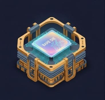
After a 12-inch wafer undergoes three months and hundreds of extremely complex photolithography and etching processes at TSMC, the tiny silver squares with metallic luster, cut by a diamond blade, have a unique and stark industry term: "Bare Die".
To the layman, a bare die is the crystallization of technology; but to engineers, at this stage, the bare die is desperately fragile.
To enable the tens of billions of transistors within a 3nm chip to operate at extreme speeds without mutual interference, TSMC must fill the spaces between metal interconnects with an insulating material called Low-k (low dielectric constant). To reduce the dielectric constant, the most direct method is to "introduce countless microscopic pores into the material." This leads to a fatal side effect: the interior of an advanced bare die resembles a nano-scale "soda cracker." It is extremely porous and brittle. If you attempt to pick it up with tweezers or press it directly onto a motherboard, even a mechanical stress of just a few tens of grams will instantly shatter (Crack) the bare die's internal microstructure, rendering the entire chip immediately unusable.
For a bare die to communicate with the outside world, it must do so through tiny metal contact points (Pads or Micro-bumps) on its surface. These metal contacts are extremely small, and if directly exposed to an ordinary atmospheric environment, oxygen and moisture in the air will chemically react with the metal "within seconds," immediately forming an extremely thin oxide layer on the surface. In daily life, a rusty nail might not be a big deal; but in the world of semiconductors, this oxide layer is sufficient to completely block the extremely weak and high-speed currents and signals of an AI chip.
Bare dies are extremely sensitive to light and dust. A tiny speck of dust in the real environment, landing on the nano-scale chip surface, is like a giant meteorite crashing onto a highway, directly crushing the circuitry; and exposure to ordinary light can even trigger unexpected photoelectric effects, generating random electrons that interfere with the chip's logical operations.
Strategic Insight: The Philosophical Duel of Soul and Body
Understanding the fragility of a bare die allows us to provide the most precise definition of "semiconductor manufacturing":
- Frontend (wafer fabrication), represented by TSMC, is essentially about bestowing a "soul" upon the chip. It instills powerful logical processing capabilities with billions of transistors, but this soul lacks physical protection; it dies upon exposure to light and cannot be touched.
- Meanwhile, Backend (packaging and testing), represented by OSAT companies like ASE, is essentially about creating a "physical body" for this fragile soul, enabling it to survive and operate in the real physical world.
Without TSMC, AI lacks intelligence; but without packaging and testing companies, AI wouldn't even be able to survive.
This is why bare dies must be sent to packaging facilities. However, it's crucial to note that in the era of AI chips, packaging is definitely no longer as simple as "putting on a black plastic protective casing." It is a physical war involving extreme currents, nuclear bomb-level heat, and massive data transmission.
This "physical body" must bear the "Four Sacred Tasks" that determine the chip's life or death.
Chapter 2: Building the Strongest Powered Armor: The "Four Sacred Tasks" of Packaging
To the layman, packaging is like putting a black plastic protective shell on a chip; but on the battlefield of AI and advanced processes, this "plastic shell" is actually an extremely expensive, technologically dense "micro-powered armor."
When that fragile bare die is sent to the packaging facility, it's like an infant with top-tier intelligence but no ability to survive. Packaging and testing (OSAT) companies must, through a series of extremely complex material science and precision mechanics, endow it with four life-or-death tasks. If even one fails, an AI chip worth tens of thousands of dollars instantly becomes industrial waste.
We have a misconception about electronic products: the smaller the chip, the less power it consumes. But in the world of AI computing, this common knowledge is completely inverted.
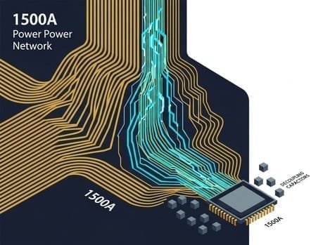
Let's do a simple and brutal junior high school physics problem ($P=IV$, Power = Current \times Voltage).
A top-tier AI chip (such as NVIDIA's latest architecture) can reach a full-speed operating power consumption (TDP) of over 1000W to 1200W. For comparison, the microwave oven or induction cooker you use at home to heat water is roughly in this wattage range.
But here's the problem: to enable the tens of billions of transistors inside a 3nm chip to switch at extreme speeds without burning out, TSMC must lower the chip's operating voltage very significantly, typically between 0.7V and 0.8V.
Divide 1200W of power by 0.8V of voltage, and you'll get an extremely terrifying number: 1500 Amperes!
What does 1500 Amperes mean? An industrial heavy-duty welder, used to fuse two thick steel plates together, only requires 200 to 300 Amperes of current. And now, we must stably, cleanly, and continuously feed a furious current of up to 1500 Amperes into a silicon chip just a few square centimeters in size.
This is the "First Sacred Task" of packaging. The packaging substrate (such as expensive ABF substrates) is filled with extremely complex, intricate 3D copper traces, much like the micro-capillaries in a human body. It must act like a super substation, precisely splitting the massive current from the server motherboard into tens of thousands of weak currents, evenly feeding each power delivery node on the chip.
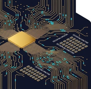
The Deadly Killer: IR Drop
In this process, the biggest enemy is "IR drop" (voltage drop). If the copper traces inside the package are too long, or the resistance is slightly too high, a mere 0.05V drop in the 0.8V voltage during transmission (turning it into 0.75V) will cause logic gates within the chip to misjudge due to insufficient voltage, leading to the entire AI server crashing (this is called Voltage Droop).
To solve this problem, packaging engineers must even densely pack tiny "decoupling capacitors" between the chip and the substrate, acting as miniature reservoirs next to the chip to instantly meet its surging current demands. Without a top-tier packaging power delivery network, an AI chip wouldn't even be able to boot up.
If power supply is the blood of the chip, then signal transmission is the chip's nervous system. This is also the core reason for the existence of all advanced packaging (including CoWoS, Flip Chip).
AI chips possess extremely strong computing power (the soul), but they themselves cannot store much; they need to constantly fetch data from adjacent memory (HBM). If the data transmission speed cannot keep up with the chip's computing speed, the GPU will be left idling, waiting – this is known in the industry as the fatal "Memory Wall."
To solve this problem, the chip must establish a massive number of I/O (input/output) connections with the outside world.
In the era of traditional wire bonding, signals were routed by individual gold wires, thinner than a human hair, from the "edge" of the chip to the substrate. This is like city traffic where all vehicles can only enter and exit through a few tollbooths at the border; once the number of I/Os exceeds a few hundred, there's no more room for any wires at the edge. Furthermore, long and thin gold wires create severe "inductance effects," turning high-frequency signals into noise during transmission.
The Ultimate War Against Distance:
The evolution of packaging technology is, in essence, a history of "eliminating physical distance."
Engineers invented flip-chip packaging, which involves flipping the chip over and populating its "entire underside" with tens of thousands of micro-bumps, pressing them directly onto the substrate, shortening the signal path from 5 millimeters to 0.1 millimeters.
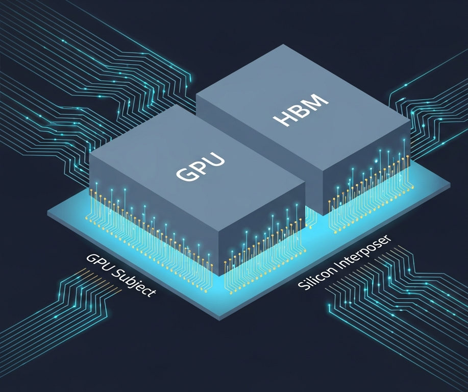
By the AI era, even the traces on ABF substrates were considered too thick and too slow. Thus, TSMC invented CoWoS, which places an extremely flat "silicon interposer" beneath the chip. Using semiconductor photolithography processes, incredibly fine tracks with line widths of only a few micrometers are drawn within the silicon interposer, allowing the GPU and HBM to achieve astonishing data speeds with bandwidths of several TB per second.
Packaging is about building the densest, speed-limit-free highway network in human history at a microscopic scale.
If current and signals successfully enter and exit, the chip then faces the most relentless punishment in physics: the second law of thermodynamics.
As mentioned earlier, an AI chip consumes 1200W of electrical energy. According to the law of conservation of energy, apart from a tiny fraction converted into transmitted signals, over 99% of this electrical energy is ultimately converted into pure "thermal energy."
Imagine concentrating 1200W of heat generation on a silicon die with an area of only about $800 \text{ mm}^2$ (not much larger than your thumbnail). Its "heat flux density" not only surpasses that of a household iron by tens of times but even approaches the core of a nuclear reactor in a nuclear power plant, or the engine nozzle of a rocket during liftoff!
If this heat is not dissipated instantly, the internal temperature of the chip can spike over 120°C in milliseconds. The chip would activate protection mechanisms due to thermal runaway, forcing it to throttle down, or even burn out entirely.
Heat Dissipation Warfare at the Packaging Level:
Do you think heat dissipation is the concern of chassis manufacturers or thermal module providers (like Sunon, Auras Technology)? Wrong, the most critical heat dissipation bottleneck is stuck "inside the package."
When heat is generated from the bare die, it must first pass through a very thin layer of Thermal Interface Material (TIM1), conduct to the metal lid or heat spreader of the package, then pass through a second layer of thermal interface material (TIM2), and finally transfer to the external liquid or air cooler.
This is precisely why in section 5-2 we will deeply highlight Promate Solutions (7751) and material distributors. If TIM1 is not applied uniformly, or if "pump-out effect" occurs under long-term high temperatures (where the thermal paste is squeezed out by thermal expansion), leading to localized dryness and the formation of microscopic air bubbles, "hotspots" will appear in localized areas of the chip, causing it to crash directly. No matter how powerful the external liquid cooling system, if the microscopic heat dissipation path inside the package is blocked, everything is futile.
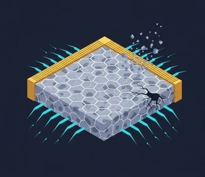
The last task, and the one that most severely tests chemical material science: protecting the fragile bare die so it can survive in the real world.
Besides moisture resistance, dust resistance, and impact resistance, the most formidable enemy packaging materials must combat is called "CTE Mismatch (Coefficient of Thermal Expansion Mismatch)."
The entire package is composed of stacked different materials: the silicon chip on top, various copper metals and chemical resins in the middle, and the PCB substrate (composed of fiberglass and resin) at the bottom.
Every time an AI chip starts running at full speed, and its temperature skyrockets from 25°C to 100°C, the nightmare of physics begins:
- The silicon chip's Coefficient of Thermal Expansion (CTE) is approximately $2.6 \text{ ppm/°C}$, meaning it expands very slowly when heated.
- However, the PCB substrate underneath has a CTE of over $15 \text{ ppm/°C}$! It expands dramatically when heated.
You can imagine a rigid, non-expanding piece of glass (silicon chip) rigidly glued to a wildly expanding plastic board (PCB substrate) underneath. What's the result?
This powerful mechanical pulling force (shear stress) will directly tear apart the micro-bumps connecting the two, or even cause the chip to severely warp and deform like a grilled squid! This is known in the industry as "Warpage."
The Salvation of Chemical Cement:
To solve this physical inferno, packaging factories must precisely inject a high-end epoxy resin called Underfill into the tiny gaps between the chip and the substrate.
This is a high-tech "micro-cement." It is filled with nano-scale silica spheres, and after being injected and cured by high-temperature baking, it firmly adheres to the chip and substrate, perfectly absorbing and uniformly dispersing the thermal expansion stress between the two, ensuring that the micro-bumps are not torn apart.
This is why, in the equipment battlefield of section 5-2, Taiwanese equipment manufacturers capable of precisely controlling baking temperatures (like Chih-Sheng Ind.) and flawlessly dispensing Underfill without bubbles (like Manz Automation) enjoy such a significant moat and market premium. This is because they are solving the most challenging physical and chemical limits in semiconductors.
Chapter 3: The Reversal of Cost Structure: When the "Plastic Protective Casing" Becomes a Gold-Devouring Behemoth
For the past three decades, the attention of foreign analysts and technology media has always been fixated on giants like TSMC and Intel, battling it out in "Frontend (wafer manufacturing)" to push Moore's Law.
In traditional perception, the semiconductor cost structure was an ironclad rule: Frontend wafer manufacturing accounted for 90% of the total chip cost, while Backend packaging and testing contributed less than 10%. OSAT (Outsourced Semiconductor Assembly and Test) companies were long regarded as "low-margin grunt work" in the semiconductor industry chain, earning profits through management efficiency and tight control over labor costs. For a chip costing a few tens of dollars, the packaging and testing quote might be just a few cents.
However, in the era of 3nm advanced processes and AI behemoth chips (such as NVIDIA B200, AMD MI300), this ironclad rule has been completely shattered.
To accomplish the aforementioned "power, signal, thermal, and protection" four sacred tasks, AI chip packaging is no longer a cheap plastic shell and gold wires; it has become an extremely expensive "system-level miniaturization engineering." The cost proportion of backend packaging and testing is rapidly and dramatically increasing, to the point where, in some extremely high-end product lines, the cost of backend packaging and materials has begun to approach the manufacturing cost of the frontend bare die itself!
This "reversal of the cost structure" primarily stems from three gold-devouring behemoths:
- Extremely Expensive High-End Substrates (ABF Substrate): Previously, substrates were like inexpensive floor tiles; now, AI chip substrates are akin to an underground subway system with 20 to 30 layers of microscopic pipelines. To support kilowatts of current and large packaging areas, the highest-end ABF substrates can even approach the size of an adult's palm. The production yield for such substrates is extremely low, with a single piece costing hundreds of dollars, directly becoming a bottomless pit for packaging costs.
- Using "Frontend Equipment" for "Backend Packaging": Traditional OSATs used wire bonders and dispensing machines. But in the era of CoWoS and SoIC, to create micron-level silicon interposers and Through-Silicon Vias (TSVs), TSMC must bring in "lithography machines (steppers)" and "etching machines," each costing hundreds of millions of New Taiwan Dollars, into the packaging facility! When packaging begins to utilize frontend wafer fab equipment like Extreme Ultraviolet (EUV) and yellow light tools, its capital expenditure and depreciation costs are already at a level that traditional OSAT companies cannot bear.
- Unbearable "Sunk Cost": If traditional wire bonding fails, you only lose a power management IC worth a couple of dollars. But if, in the final step of CoWoS packaging, the chip warps and is scrapped due to uncontrolled temperature, you instantly lose a 3nm GPU bare die worth thousands of dollars, plus four to eight extremely expensive HBM (High Bandwidth Memory) modules. This fear of "tens of thousands of dollars turning to zero overnight" drives up the value of high-end testing and inspection equipment.
This is precisely why TSMC (Foundry) absolutely cannot hand over AI chip packaging to traditional OSAT companies.
When packaging technology has become the absolute bottleneck determining whether an AI chip "can survive" and "how fast its computing speed can soar," TSMC's logic is simple: "My customers (NVIDIA/AMD) need top-tier packaging to unleash the computing power of 3nm. Since traditional OSATs can't do it, I'll step in and do it myself!"
The traditional demarcation line between frontend and backend has officially disappeared. Packaging has formally transitioned from a "cost-reducing supporting role" to a "new main battlefield" that determines chip performance, binds super-customers, and creates extreme gross margins.
However, all this expensive packaging magic has a major prerequisite – you must ensure that the bare die you put in is completely intact.
If the bare die itself is flawed, dressing it in the most premium golden armor will still make it useless. This leads to the next and most brutal challenge in advanced packaging, one that severely tests capital logic: before spending a fortune on packaging, how do we use "testing" to determine a chip's life or death and its quality tier?
In-depth Research · Quantitative Perspective
Want to gain more insights into semiconductor quantitative research?
【Insight Subscription Plan】Break Free from Retail Investor Mentality: Build Your Alpha Trading System with "Quantitative Chips" and "Consensus Data"EDGE Semiconductor Research
📍 Series Map — Navigate the Complete EDGE Semiconductor Research →


