Chapter Focus: In the era of advanced processes and AI chips, "testing" is not traditional QA. Instead, it is a **capital allocation tool** used to **prevent the expansion of sunk costs** and to **maximize the gross margin of an entire wafer** through **Binning**.
1) Testing is Not QA: It's a Cash Flow Breakwater
Before we send the fragile bare die fabricated by TSMC into an expensive "power armor (advanced packaging)", we must first ask a multi-billion dollar question: "Are you sure this chip's 'soul' is normal?"
Many investors new to semiconductors, and even some tech media, often misunderstand semiconductor testing as merely a QA (Quality Assurance) spot check similar to an iPhone assembly plant—checking for scratches on the exterior or if it powers on.
Completely wrong! In the relentless battlefield of advanced processes and AI chips, testing is absolutely not simple quality control or defect detection.
It is an "extreme capital allocation tool," and even more, the strongest breakwater used by semiconductor giants to protect their cash flow.
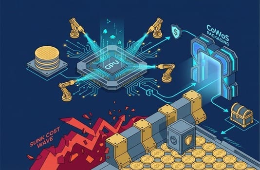
2) 💸 The Extreme Fear of Sunk Costs: Slamming the Brakes Before Burning Cash
To understand this business logic, we must calculate a very cruel "sunk cost" math problem.
In the era of mature processes (e.g., 28nm for TV remote control chips), a chip was cheap like cabbage. If a chip was faulty, even if it was accidentally packaged before being discovered as unusable, the loss would typically be only a few dollars. It would be discarded as trash, and even the cost of the test equipment might be higher than the chip itself.
However, in the world of AI chips, the rules of the game have completely changed.
Imagine TSMC baking a 12-inch wafer for NVIDIA or AMD using the most cutting-edge 5nm or 3nm process. After dicing, the "pure manufacturing cost" of a large GPU bare die alone could be as high as over $500 USD.
If we don't conduct strict CP testing (Circuit Probing, wafer-level probe testing), or if we test carelessly to save money, and directly send this chip to the next stage—which is currently the most scarce and precious capacity in the world: CoWoS advanced packaging.
What will happen next?
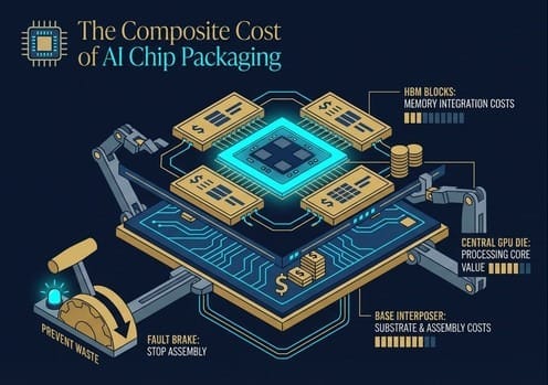
- Stacking of Packaging Costs: This chip will be placed on an expensive Silicon Interposer, an action that will burn at least another $200 to $300 USD.
- Collateral Damage: To form a complete AI computing unit, this GPU must be bound with 4 or even 8 extremely expensive HBMs (High Bandwidth Memory), which adds several hundred more dollars in cost.
When the entire CoWoS package is completed, this complex, now valued at over $1000 USD, is sent to the test machine. Upon powering up—"Snap!"—a tiny nanoline short circuit is found inside the GPU.
Congratulations, the total cost of over $1000 USD instantly vanishes.
This is not even the worst part. In today's AI capacity shortage, you lose not only money, but you also unnecessarily occupied TSMC's extremely scarce CoWoS capacity, as well as the HBM laboriously produced by SK Hynix. If Jensen Huang knew you were using faulty chips to occupy his CoWoS capacity, he would be furious.
This is why "testing" has become so sacrosanct in advanced processes.
Before the wafer is cut and expensive packaging is applied, the sole mission of test machines and probe cards is to subject these bare dies to various extreme voltages and signals, finding even one in ten thousand defects.
In summary, the purpose of CP: Faced with the final price of AI chips, often tens of thousands of dollars, the ultimate goal of wafer testing (CP) is only one—
Slamming the brakes hard before throwing large sums of money into the packaging plant, picking out and discarding the bad apples, and not allowing a single penny of packaging cost to be wasted on them.
This is not engineering; this is pure financial risk control.
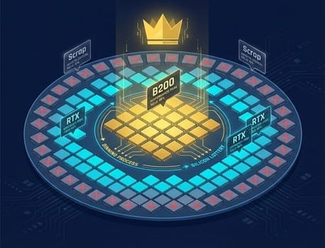
3) 👑 The Power of the Kingmaker: Binning and the Silicon Lottery
If you thought the test machine's screen only displayed "Pass" and "Fail," then you've missed the most powerful black technology semiconductor giants use to manipulate gross margins.
In the microscopic world of AI and HPC (High-Performance Computing) chips, a very counter-intuitive truth exists: chips are not absolutely "good" or "bad"; there are only "differences in physical quality."
When TSMC sends a 12-inch wafer into a high-temperature furnace and subjects it to hundreds of chemical and physical tortures, the hundreds of chips on this wafer are not identical clones. Due to edge stress, minute differences in photoresist coating thickness, or etching concentration, chips near the "center" of the wafer usually have excellent physical quality, while chips closer to the "edges" may be slightly worse.
This is jokingly referred to in the industry as the "Silicon Lottery." With the same design and the same process, some chips can run at incredibly high computing clocks (frequencies) with extremely low voltage and without overheating; some chips will experience rampant leakage as soon as the frequency is raised, leading to instantaneous temperature runaway; and some chips may even have 2 out of 100 internal computing cores that are inherently disabled.
Faced with this physical variation, should all those slightly imperfect but expensive chips be simply discarded as trash?
Absolutely not! At this point, the wafer test machine (CP Test) becomes the "Kingmaker" that determines a chip's class for life.
Through extreme interrogation by probe cards and test machines, engineers will perform "Binning" on each chip on the wafer:
- 🏆 Top Tier Quality (Tier 1): Heir to the Golden Throne
- These chips are flawless, with extremely low voltage, extremely high clock speeds, and minimal leakage.
- They will receive tickets to the most prestigious CoWoS packaging, equipped with the top-tier 8 HBM3e memories.
- Ultimately branded as NVIDIA B200 or AMD MI300X, sold at sky-high prices of tens of thousands of dollars to hyperscale data centers like Microsoft, Meta, or Google.
- 🥈 Second Tier Quality (Tier 2): Standard Troops with Down-Tiering
- What if a chip has a few broken cores, or overheats too easily during high-frequency operation?
- The test machine will issue instructions to "permanently seal off" those broken cores, either by physical laser fusing or software masking, and lock the maximum operating frequency to a safe zone.
- Then, this chip will be downgraded and labeled as a "lower-tier model" (e.g., the consumer-grade graphics card RTX 4080 is actually an RTX 4090 with some cores disabled; or sold as a de-specified AI chip for enterprise). It can still fetch thousands of dollars, without wasting a single penny on R&D.
- 💀 Inferior Quality (Tier 3): Directly Scrapped Death Row Inmate
- Only a very small number of chips that cannot even conduct the most basic logic gates, or have such severe leakage that they might burn out the motherboard upon powering up, will be ruthlessly marked with a red "X" and sent directly to the scrap bin.
Do you understand now? This is the true business value of test equipment.
Test machines and probe cards are not just looking for bad apples. They are helping to precisely label each apple on the entire wafer with different prices, achieving "maximum extraction of residual value," pushing the gross margin of the entire wafer to its absolute maximum.
Without strong binning capabilities, NVIDIA would not be able to precisely segment so many product lines with different price points and computing powers to capture the entire market.
However, when the test machine confidently sorts these chips into classes, is the judgment over?
No.
Within the physics of semiconductors lies a "curse" that even the most powerful test machine cannot overcome. This will directly lead us to the truth behind the massive overflow orders received by test equipment manufacturers (such as Chroma, Hongjin).
4) ⏳ Extreme Suspense: The Counter-Intuitive "Uncertainty Principle" and the Curse of Time
When the probe card slowly lifts from the 12-inch wafer, and the test machine screen flashes the "Tier 1 Pass" green light, indicating the highest grade, can engineers breathe a sigh of relief and directly package this perfect 3nm GPU bare die to send to NVIDIA or AMD?
The answer is: Absolutely not.
Because in the physical world of semiconductors, there exists an extremely counter-intuitive "uncertainty principle" that makes all OSAT (Outsourced Semiconductor Assembly and Test) companies shudder.
The "uncertainty" here is not Schrödinger's cat from quantum mechanics, but a very real commercial and physical pain point:
Wafer-level testing (CP Test, Circuit Probing) can never accurately predict a chip's "future."
Although wafer testing (CP) is precise, it is essentially a "static health check." It is usually performed at room temperature (around 25°C) or slightly elevated temperatures, and the test time is only a few seconds to tens of seconds. It can only tell you: "This chip, at 'this very moment,' at 'normal temperature,' has functioning logic gates and normal voltage."
But the true battlefield for AI chips is not a cleanroom at a constant 25°C. They will be installed in hyperscale data centers of Microsoft, Meta, or Amazon, processing trillion-parameter large language models (LLMs) day and night.
In the real battlefield, there are two invisible "micro assassins" that can cause "perfect chips" that scored full marks in CP testing to fail instantly after packaging or even after shipment.
4-1) 🗡️ Micro Assassin One: The Thermodynamics Demon (High-Temperature Leakage and Thermal Crash)
As we mentioned in the previous section, chips manufactured by wafer fabs vary in physical quality. Some chips' transistor gate oxides (the insulating layer controlling current switching) might be a few tenths of a nanometer thinner than the standard during photolithography.
On a 25°C CP test machine, this tiny defect does not affect operation at all. Current is properly blocked, and the chip successfully passes the test.
However, when this chip is packaged and placed in a server, with AI computing running at full throttle, the chip's temperature rapidly soars to 90°C or even 105°C within seconds, and then a terrifying event occurs.
The laws of physics tell us: semiconductor leakage current increases "exponentially" with rising temperature.
That slightly thinner insulating layer, at a high temperature of 105°C, can no longer hold back the rampant electrons. Electrons begin to penetrate the insulating layer in large numbers, causing severe leakage. This leakage generates more waste heat, which in turn causes even more severe leakage—a phenomenon known in the industry as "thermal runaway." Ultimately, the chip directly crashes due to overheating in the server, or even burns a hole in the motherboard.
This is the blind spot of CP test machines: they do not have the time or the environment to simulate the dynamic collapse process of a chip under extreme high temperatures.
4-2) 🗡️ Micro Assassin Two: The Curse of Time — Electromigration (EM) and Latent Defects
If high temperature is an immediate killer, then the second assassin is a slow-acting poison. This is also the ultimate demon that AI chips fear most: Latent Defects and Electromigration (EM).
What is electromigration? Imagine a microscopic copper wire, only a few nanometers wide. When an AI chip operates at full speed, an extremely large current (as we calculated earlier, up to thousands of amperes) is squeezed into this extremely narrow wire. These high-speed electrons are like a furious "electron hurricane." As the "electron wind" continuously strikes the metal atoms in the copper wire, it "physically pushes" the metal atoms away.
Day after day, month after month. The originally smooth copper wire:
- In some places, metal atoms are hollowed out, forming "voids," leading to soaring resistance or even an open circuit.
- In other places, metal atoms accumulate into "hillocks," puncturing the insulating layer and causing a short circuit with adjacent wires.
This is the horror of electromigration: it requires "time accumulation" to manifest.
Some chips may have an extremely tiny scratch or bubble on a wire during manufacturing (this is a latent defect). During CP testing at the factory, this wire can still conduct electricity, and signals are completely normal.
However, when this chip is sold to Google and runs continuously in a data center for three months, this tiny bubble, under the incessant erosion of the electron wind, finally expands into a huge void.
"Snap!" goes the sound. An AI server worth millions of New Taiwan Dollars unexpectedly crashes late one night, causing cloud service disruptions.
Leverage Effect of Risk (Downstream Failure Cost)
- If this chip is caught and discarded within the TSMC fab (CP test), the loss is $500 USD.
- If it is discovered to be faulty after packaging, the loss is $1500 USD.
- If it is sold to a client, leading to field failure, cabinet downtime, cloud service interruption, dispatching maintenance, and reputational compensation, the loss can reach hundreds of thousands or even millions of USD.
5) ⛓️ The Birth of Purgatory: Why Test Equipment Manufacturers Are Entering a Golden Age?
It is precisely because of this cruel "uncertainty principle," and because CP testing cannot detect high-temperature thermal runaway and latent defects, that tech giants like NVIDIA, AMD, and Apple are forced to invest astronomical sums to establish layer after layer of "ultimate purgatory (Downstream Testing)" after chip packaging is completed.
This perfectly explains why, in the upcoming 5-4 combat zone, we will see the rapid rise of the following equipment manufacturers in Taiwan's stock market:
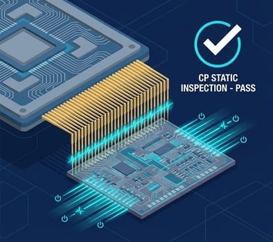
- Post-Packaging Comprehensive Check-up — FT Test (Final Test)
- After the chip dons its power armor, we must reconfirm that this armor (packaging lines) has no short circuits.
- Since the chip now has pins, we cannot use probe cards. We must use extremely expensive "sockets" that can withstand extremely high-frequency signals without distortion.
- This explains the highly profitable logic behind WinWay Technology (6515)'s coaxial test sockets, which can sell for over ten thousand USD per unit.
- The Torture Chamber of the Time Machine — Burn-in Test
- To catch latent defects that only manifest "three months later," we cannot wait three months.
- Engineers invented Burn-in ovens: tens of thousands of dollars worth of GPUs are sent into a hellish sauna at up to 125°C, simultaneously subjected to extreme high voltage, and "baked" for days and nights.
- This is called "stress-accelerated aging." We want to prematurely kill off chips with weak physical quality and latent defects right in the factory.
- This has made HongJing Technology (7769), which masters high and low-temperature automated handling equipment, an infrastructure provider in the AI era.
- The Final Exam of the Real Battlefield — System Level Test (SLT)
- Even after passing Burn-in, NVIDIA is still not at ease.
- In the final stage, we no longer test voltage and current. We directly plug the AI chip into a real motherboard, install a Linux operating system, and run actual large language models (LLM) for several hours to see if it crashes.
- During these few hours, the chip's temperature will fluctuate wildly. We need divine equipment that can precisely inject water for temperature control within 50 milliseconds.
- This is the absolute monopolistic moat built by Chroma (2360).
Conclusion: This is an Extreme Tug-of-War Between Time and Cost
In the past, testing a consumer-grade chip took only 3 seconds.
Now, testing an AI chip, from CP, FT, Burn-in to SLT, takes a total of several hours or even days.
When "test time" increases by a hundredfold, the demand for test machines follows with a hundredfold increase.
This is not a cyclical recovery; this is a "structural rigid demand" driven by the physical limits of semiconductors.
In-depth Research · Quantitative Perspective
Want more quantitative research insights on semiconductors?
[Insight Subscription Plan] Bid Farewell to Retail Investor Mentality: Build Your Alpha Trading System with 'Quantitative Capital Flows' and 'Consensus Data'EDGE Semiconductor Research
📍 Series Map — Navigate the Complete EDGE Semiconductor Research →


