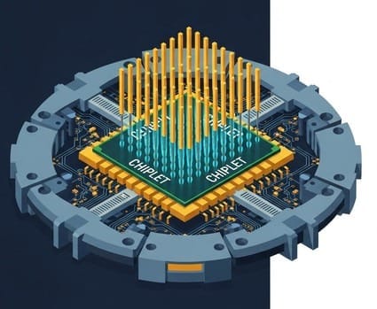
Chiplets turn packaging yield into a "multiplication" problem, forcing the industry to pursue KGD (Known Good Die).
The prerequisite for KGD is extreme wafer testing capability, and probe cards are the critical interface that "injects" signals and current.
In the era of 112G and even 224G high frequencies, traditional probe length causes inductance and antenna effects, making MEMS probe cards mainstream.
MPI Corporation (6223) adopts an "all-encompassing scale" approach, while Chunghwa Precision Test Technology (6510) pursues a "pure high-frequency" route, forming a duopoly.
Era Background: From Monolithic to Chiplet
In the traditional semiconductor era, TSMC manufactured chips using a method called "monolithic." This involved cramming all computing cores, memory controllers, and I/O interfaces into a single, increasingly larger silicon die.
However, with the insatiable explosion in demand for AI computing power, this path has reached its limit. If the next-generation AI chip were to be made as large as a palm, a single speck of dust falling on the wafer would render the entire massive chip scrap, leading to yields so low that NVIDIA would go bankrupt.
Thus, the semiconductor industry ushered in a historic architectural revolution: the "Chiplet Era."
Engineers began to break down the originally enormous chips into several smaller chiplets (e.g., manufacturing the CPU, GPU, and SRAM separately). These were then assembled tightly onto a single substrate, much like building with LEGO bricks, using TSMC's advanced packaging technologies (such as CoWoS or SoIC).
This sounds like a perfect plan for cost reduction and efficiency improvement, doesn't it?
Wrong. For OSATs (Outsourced Semiconductor Assembly and Test), Chiplets are nothing short of a Russian roulette gamble on yield.
🎲 The Deadly Multiplication Effect: The Destructive Cost of One Bad Apple
In the world of Chiplets, a mathematical law exists that makes all packaging engineers break out in a cold sweat—the "Yield Multiplication Effect."
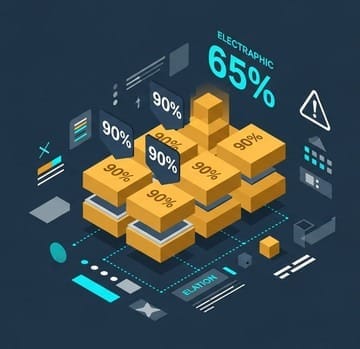
Let's do a simple math problem. Suppose we need to package four small chiplets together to form a powerful AI processor. Before packaging, the manufacturing yield of each of these four chiplets at the wafer fab is as high as 90%.
Sounds excellent, right? A 90% yield is already exemplary in traditional manufacturing.
But when you package them together, what will be the yield of the final product?
Is it 90%? No.
Is it $(90\% + 90\% + 90\% + 90\%) / 4 = 90\%$? Not exactly.
The true mathematical formula is:
That's right, the final packaging yield instantly collapses to just 65%!
This is just the case for stacking four chiplets. If we look at NVIDIA's upcoming architectures, they often involve two GPUs paired with eight or even twelve HBMs (High Bandwidth Memory). When you stack more than ten chiplets together, even a slight drop in the yield of a single chiplet will cause the overall composite yield to exhibit a "cliff-like exponential collapse."
Under the guilt-by-association principle of advanced packaging, if just one chiplet is bad, it will act like a single bad apple, dragging down all the surrounding perfect, extremely expensive good chiplets, along with the costly silicon interposer beneath them, to their demise!
This entire AI composite, valued at tens of thousands of US dollars, will directly become industrial waste.
🛡️ KGD (Known Good Die)'s Extreme Demands
Once you understand this cruel multiplication effect, you'll grasp why, in the Chiplet era, the entire semiconductor industry chain is frantically pursuing one term: KGD (Known Good Die).
"Probably good" or "95% yield" are not acceptable phrases in advanced packaging factories.
Before TSMC and ASE's packaging machines bond a chiplet, they must be 100% absolutely certain that it is perfect. Without the guarantee of KGD, the Chiplet business model simply cannot work, and the packaging factory's gross margin would be instantly devoured by astronomical compensation costs.
However, here's the problem.
This chip has yet to be packaged; it doesn't have long pins. It only has densely packed, microscopic metal aluminum pads, smaller than bacteria, on its surface.
How do we inject high-frequency signals and violent currents into it to confirm that it is a 100% perfect KGD?
This requires the entry of the semiconductor testing stage's most precise, most aggressive, and highest-gross-margin "microscopic assassin."
⚔️ Microscopic Assassin: The Physical Purgatory of Probe Cards
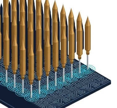
If we were to visualize what a "probe card" looks like, you could imagine a specialized, high-end printed circuit board (PCB) about the size of a frisbee. But in the exact center of this circuit board's bottom, a core mechanism called a "Probe Head" is embedded.
On this probe head, an area of just a few square centimeters, thousands or even tens of thousands of hair-thin metal microneedles are densely arranged. It is truly a "microscopic sword mountain."
In the cleanroom for wafer testing (CP Test), the test machine clamps this probe card, aligns it with the underlying 12-inch wafer valued at tens of thousands of US dollars, and then relentlessly presses down.
This action is known in the semiconductor industry as "Touchdown."
This is an extremely violent microscopic physical process. Every microneedle on the probe card must be aligned perfectly with each metal aluminum pad on the chip with micrometer ($\mu m$, one-millionth of a meter) precision.
The moment the probe presses down, it must possess extremely precise "elasticity and overdrive."
If pressed too lightly: The probe tip cannot penetrate the microscopic oxide layer that instantly forms on the aluminum pad's surface in the air. Current cannot be injected, and a perfectly good chip will be mistakenly identified as a bad one (false fail).
If pressed too heavily: The sharp probe tip will directly pierce the aluminum pad, or even, like an awl, crush the "Low-k dielectric layer, as brittle as a soda cracker" that we mentioned in 5-1-1! This chip is instantly scrapped (overkill).
Even more terrifying is "Planarity." The height deviation of the tips of these tens of thousands of microneedles cannot exceed a few micrometers. If just a few needles are slightly shorter, the signal in that area will be interrupted.
To have tens of thousands of fine metal needles simultaneously and uniformly pierce a wafer in a high-temperature test environment of 100°C or even 125°C, without any displacement caused by thermal expansion, is almost challenging the physical limits of human precision machining and materials metallurgy.
This is precisely why only a handful of companies globally can successfully produce high-end probe cards. It's definitely not as simple as soldering a few wires onto a circuit board.
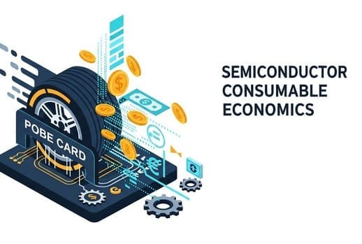
🏎️ Consumable Economics: The F1 Racing Tire Cash Cow Model
Having understood the physical purgatory of probe cards, we will now delve into the core reason why foreign institutional investors are so wildly enthusiastic about them: extremely lucrative "consumable economics."
Many investors mistakenly equate probe cards with general semiconductor equipment (such as ASML's EUV lithography machines or Applied Materials' thin-film deposition equipment). This is a completely flawed valuation logic.
General capital equipment is sold one unit at a time; customers purchase it and can depreciate it over ten or eight years, and the equipment manufacturer only earns meager maintenance and servicing fees.
But probe cards are different. Probe cards are the "F1 racing tires" of test machines.
Imagine F1 racing tires: they must withstand extreme grip, ultra-high temperatures, and intense friction. After a few dozen laps at full speed on the track, the tire rubber will be completely worn smooth. If the car doesn't pit immediately for a tire change, it will lose control and crash.
The fate of probe cards is exactly the same.
In test houses (such as King Yuan Electronics or ASE), test machines operate 24 hours a day, non-stop. The microneedles of a probe card perform a "Touchdown" on the hard silicon wafer every few seconds.
Accompanied by the extreme test currents of AI chips, reaching hundreds or even thousands of watts, the probe tips generate high temperatures. Coupled with repeated mechanical collisions, the probe tips gradually wear down, become dull, or even bend and deform due to metal fatigue. Additionally, when piercing the aluminum pad's oxide layer, the probe tips pick up tiny metal fragments, which over time can cause electrical resistance to spike.
According to industry standards, after a high-end probe card experiences 100,000 to 500,000 Touchdowns, its physical lifespan reaches its limit. Like worn-out F1 tires, it must be scrapped and replaced directly, or sent back to the original manufacturer for extremely expensive probe head reconstruction (Re-build).
If an OSAT's machines operate at full capacity, a single probe card might be completely consumed within a few months or even a few weeks!
This is the unique "Razor and Blades Model" of probe card manufacturers:
Astronomical Unit Price: To test NVIDIA's or AMD's latest generation of massive AI chips, a top-tier probe card with tens of thousands of microneedles can cost up to $100,000 to $200,000 USD (equivalent to TWD 3 million to 6 million)! This is the price of a single "consumable component"!
Endless Recurring Orders: As long as TSMC's wafers continue to be produced and NVIDIA's chips continue to be updated, customers must dutifully place orders for "new tires" with probe card manufacturers every month and every quarter. This represents extremely stable recurring revenue.
Peak Gross Margins: Due to extremely high technical barriers, and because customers would never dare to save a few tens of thousands of dollars by buying unbranded probe cards (who would compensate if multi-million dollar wafers were damaged?), this grants probe card manufacturers strong pricing power. High-end probe cards consistently maintain gross margins of 45% to over 50%.
This is a premium business that collects "tolls." This is precisely the underlying capital logic why MPI Corporation (6223) and Chunghwa Precision Test Technology (6510) enjoy such high valuations in the Taiwan Stock Exchange.
⚡ Probe Metallurgy and MEMS Revolution: The Nonlinear Collapse of Frequency
For the past few decades, probe card manufacturing relied heavily on "advanced handicraft." Traditional Cantilever Probe Cards (CPC) and early Vertical Probe Cards (VPC) were assembled by highly precise automated machinery or skilled technicians who bent individual tungsten alloy wires into specific angles and then inserted and assembled them onto a substrate.
This was akin to master Swiss watchmakers meticulously assembling intricate mechanical watches.
When testing mobile phone chips or power management ICs, these "assembled" probe cards worked perfectly. However, when the test subject became NVIDIA's B200 or high-speed network switch chips, these "watchmakers" were utterly stumped.
The culprit that killed traditional probe cards is "high-frequency electromagnetics."
To address the massive data transmission bottlenecks, the I/O signal transmission speed for AI chips is escalating at a frantic pace. From earlier 28G and 56G, it has now surged to the 112G PAM4 standard for AI servers (with the next generation already eyeing 224G).
When electrical signal frequencies reach as high as 112G (meaning the signal flips hundreds of billions of times per second), the demons of fundamental physics emerge: "Inductance Effect" and "Antenna Effect."
At such extreme high frequencies, a metal conductor is no longer merely a conductor. If the probe is too long, it instantly becomes a "broadcast antenna"! High-frequency signals passing through the probe will generate strong electromagnetic radiation and interfere with an adjacent probe just tens of micrometers away. This is known in engineering as the deadly "Cross-talk."
The test machine initially expects to receive clean "0 and 1" digital signals from the chip. However, due to probe interference, the machine receives a waveform filled with static and noise (closed eye diagram).
This is an unforgiving and uncompromising physical law: when signals accelerate to 112G PAM4, even an extra 1 millimeter (1mm) in probe length will cause a "nonlinear collapse" in signal integrity!
Let's look back at traditional cantilever and vertical probes. Because they are assembled by mechanical bending, to maintain elasticity, their lengths often reach 5 to 10 millimeters. In the face of 112G high-frequency signals, testing with such probes is like trying to transmit a high-pressure water jet through a rusty, leaky iron pipe; the signal is completely destroyed before it even reaches the test machine.
Traditional assembled probe cards have officially been sentenced to death by AI chips.
To salvage high-frequency testing for 112G and even 224G, humanity must abandon "mechanical assembly" and turn to a radical dimensionality reduction attack—MEMS (Micro-Electro-Mechanical Systems) probe cards.
What are MEMS probe cards? Simply put, it's about "manufacturing probes using the same methods as manufacturing semiconductor chips."
Engineers no longer use pliers to bend tungsten wires. They've brought out the "photolithography machines," "etching machines," and "electroplating tanks" from wafer fabs. Through yellow-light photolithography and 3D electroplating technology, thousands of probes are "grown" layer by layer, atom by atom, on a substrate!
This MEMS revolution brings three overwhelming advantages:
Ultimate Miniaturization (Breaking the 1mm Curse): Because they are fabricated using semiconductor processes, MEMS probes can be made extremely short. Probe length can be directly compressed to millimeter or even micrometer levels, perfectly eliminating high-frequency inductance and antenna effects, allowing 112G high-speed signals to pass unimpeded.
God-tier Consistency: No matter how precise mechanical assembly is, ten thousand needles will inevitably have a few micrometers of error. But MEMS probes are formed in a single exposure; the ten thousand probes on them are like clones etched from the same mold, achieving 100% perfect consistency in shape, length, and elastic coefficient.
Complex 3D Electromagnetic Shielding: Through 3D electroplating, engineers can even "grow" ground shielding structures directly next to each signal probe. This is like equipping each microneedle with bulletproof armor, completely isolating electromagnetic crosstalk from adjacent probes.
Understanding this evolution of technological history reveals one thing: high-end probe cards are not merely a "precision machinery industry"; they are, without a doubt, a "semiconductor front-end manufacturing industry" combined with "high-frequency electromagnetic metallurgy"!
Globally, only FormFactor (US) and MJC (Japan) were initially capable of overcoming this formidable technological chasm. But now, two extremely formidable companies in Taiwan are fiercely competing for this premium market share, previously dominated by international giants, each with a distinct strategy.
To survive amidst the challenges from international giants FormFactor (U.S.) and MJC (Japan), and even to aggressively seize high-end market share from them, probe card manufacturers in Taiwan must find their absolute survival strategies. MPI Corporation (6223) has chosen an extremely dominant path, akin to the "Toyota" strategy in the automotive industry, for all-encompassing market leadership.
Origin and Transformation: A Manufacturing Giant Rising from the Bottom
Looking back at MPI Corporation's development history, it wasn't born with an AI silver spoon. In its early days, MPI Corporation started with LED testing equipment and traditional cantilever probe cards (CPC), which had relatively lower technical barriers, specializing in catering to the massive demand for display driver ICs (DDIC) and consumer electronics.
However, this history of "starting from the bottom" is precisely MPI Corporation's most formidable moat today. While traditional CPC and VPC (Vertical Probe Cards) may seem outdated in the face of top-tier AI chips, they still have massive and irreplaceable essential demand in automotive chips, network communication chips, and mobile phone ICs.
Leveraging these powerful "cash cow" businesses, MPI Corporation accumulated the formidable economies of scale of a top-five global probe card manufacturer and extremely deep customer stickiness. With ample cash and significant room for error, MPI Corporation dared to boldly invest vast resources into the most expensive and difficult area: MEMS (Micro-Electro-Mechanical Systems) probe card R&D.
"Can make any type of car, has every type of customer, the largest volume, the most stable production capacity." This is MPI Corporation's Toyota strategy. It not only targets the most cutting-edge AI but also aims to dominate peripheral microcontrollers (MCUs) and radio frequency chips (RF).
Industry Outlook: The Invisible Winner in the ASIC Wave and Peripheral Chips
Entering the AI era, MPI Corporation's strategy has reached its perfect harvesting period. Looking ahead to 2025-2026, MPI Corporation's strong growth will no longer be driven solely by GPU testing, but by two even larger underlying industry currents:
The Cloud Giants' ASIC (Application-Specific Integrated Circuit) Frenzy: To reduce their absolute reliance on NVIDIA and lower computing costs, global large Cloud Service Providers (CSPs, such as Amazon AWS, Google, Microsoft) are frantically investing in a self-developed AI chip arms race. These custom chips also require extremely precise high-frequency testing. MPI Corporation, leveraging its strong customization capabilities and production flexibility, has successfully secured large orders for ASIC projects from US-based cloud giants. This wave of testing demand driven by self-developed chips is expected to reach an extremely intensive shipping peak by mid-2026.
Dominance in GPU Peripheral Chips: In the AI server ecosystem, while computing cores (GPUs) are undoubtedly important, network switch chips and high-speed I/O control chips responsible for data transmission also face extreme challenges with frequencies doubling or even reaching 224G. MPI Corporation is aggressively capturing market share for testing these "peripheral but indispensable" high-frequency chips, forming an invisible profit defense line.
The Brutal Aesthetics of Capacity: The MEMS Arms Race
To capture these surging super orders, having technology alone is not enough; you must possess "capacity" that makes competitors despair.
This post is for subscribers only
Sign up now to read the post and get access to the full library of posts for subscribers only.