Reading Tip: This article will first perform a "physical coordinate calibration" before delving into Bumping (long bumps)'s *process objective → material evolution → supply chain power structure*.
Before diving into process details, we must first perform a "physical coordinate calibration" for our readers' minds. Semiconductor packaging officially diverges here into two distinct parallel worlds.
🚩 Declaration of Parallel Worlds: The Divide Between Traditional and Advanced Packaging
If you are packaging a low-power sensor or a simple microcontroller (MCU) for a remote control today, you can skip this Bumping (long bump) process.
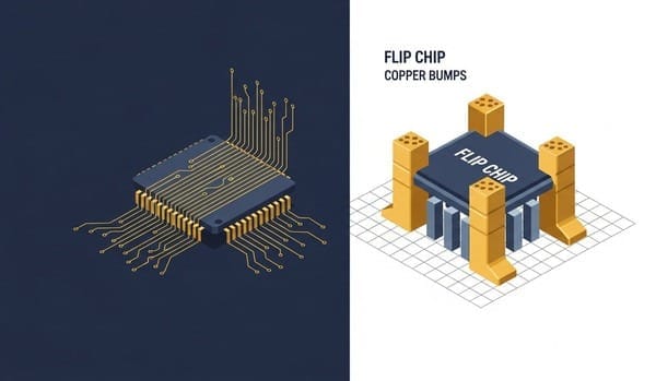
In the world of traditional packaging, wafers are directly diced after passing electrical tests, and then long gold wires (Wire Bonding) are used to connect the chip's edge contacts to the outside world. That is a "slow, low-temperature, low-cost" world.
However, if you are pursuing an AI behemoth like NVIDIA B200, which processes massive amounts of data per second and consumes over a thousand watts of power, or a flagship smartphone chip that packs the strongest computing power into a tiny space, you must enter the parallel world of "Flip Chip" or "2.5D/3D Advanced Packaging".
In this world, chips cannot be connected by "standing" and wiring; they must "lie down" and integrate directly with the substrate. To achieve this, the first and most critical step is Bumping (long bumps).
👟 Donning "Power Armor Boots" for Chips: Why Aluminum Pads Aren't Enough?
The Known Good Dies (KGD) we mentioned in 5-1-3, while having metal contacts (Pads) on their surface, these contacts are typically made of aluminum.
Although aluminum has acceptable electrical conductivity, it has two fatal physical defects that prevent it from supporting the heavy demands of advanced packaging:
- It is too soft and too thin: The aluminum pads on a bare die are only a few micrometers thick and soft. During subsequent high-pressure, high-temperature processes where the chip is "pressed into" the substrate, the thin aluminum pads would crumble like a cookie hit by a heavy hammer, directly destroying the underlying chip structure.
- It oxidizes very easily: Once aluminum pads are exposed to air, a very thin and hard layer of aluminum oxide quickly forms on their surface. This oxide layer is a non-conductive insulator, creating a huge electrical resistance barrier between the chip and the substrate.
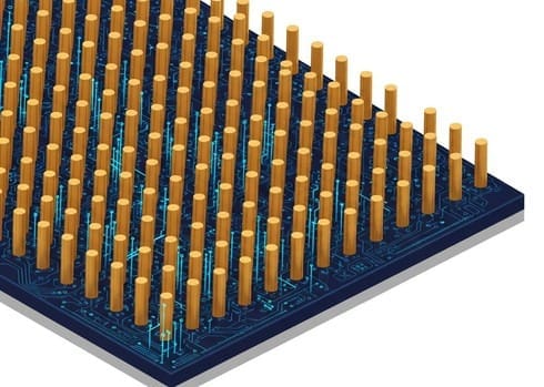
Therefore, the first task for packaging manufacturers is to "grow" spherical and hard metal bumps on these tiny, fragile aluminum pads out of thin air.
Core Analogy: This is like equipping a super athlete preparing for a 100-meter sprint with a pair of specialized "power armor boots" covered in metal studs.
These Bumps not only possess excellent electrical conductivity but also serve as "physical support," ensuring the chip remains stable during flipping, pressing down, and long-term operation through thermal expansion and contraction cycles.
⚔️ Interface War of Foundry Giants: TSMC APTS and ASE's Dominance
Behind this "shoe-fitting operation" lies the fiercest power struggle between semiconductor manufacturing and outsourced semiconductor assembly and test (OSAT).
In the past, the creation of long bumps was considered a labor-intensive task for OSATs. However, as the precision requirements for AI chips entered the micrometer level, foundries discovered that:
- If this process step is not completed within their own fabs, the yield of subsequent 2.5D advanced packaging cannot be guaranteed.
TSMC has long regarded Bumping as a core component of its "one-stop shop" service. Within TSMC's Advanced Packaging and Testing Services (APTS) facilities, wafers undergo Bumping immediately after emerging from the front-end process.
This allows TSMC to define the most stringent bump specifications (e.g., reducing pitch from 100 micrometers to tens of micrometers), directly controlling the entry ticket to advanced packaging.
As the global leader in outsourced semiconductor assembly and test (OSAT), ASE has built an insurmountable Great Wall in Bumping capacity. For customers who do not rely on TSMC's one-stop service, or who require cost-effective Flip Chip packaging (such as most smartphone and automotive chips), ASE provides the world's largest Bumping "operating table."
Capacity Background: According to supply chain surveys and institutional data, TSMC's CoWoS capacity is expected to reach 110,000 to 120,000 wafers per month by the end of 2026, with an annual growth rate exceeding 60%.
Behind this massive capacity expansion, each wafer must first undergo an hours-long "chemical plating and etching" ordeal before those millions of precise "microscopic shoes" can be grown.
However, the most exciting part of this operation is not its scale, but its "materials."
To achieve lower transmission latency and faster heat dissipation for AI chips, these "microscopic shoes" are undergoing an evolutionary transformation from tin-lead to copper pillars (Cu Pillar). This evolution has also simultaneously ushered in a golden age of high gross margins for two "wet process equipment suppliers" in the Taiwan stock market.
🧬 Violent Evolution of Materials: From "Meatballs" to "Reinforced Concrete"
In the evolution of advanced packaging, the evolution of metal bumps is essentially a natural selection against the limits of physical space and thermodynamics.
In the Flip Chip era of the past decade or so, we used tin-lead alloy balls known as "C4." These were like placing tiny "meatballs" on the chip contacts.
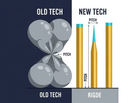
- Fatal Flaw: When the number of contacts required by AI chips surged from hundreds to tens of thousands, these "meatballs" had to be squeezed into extremely narrow spaces.
- During the reflow soldering process, the soft tin balls would deform when heated, causing adjacent balls to stick together and short-circuit.
- This is known in the industry as the "Bridging" disaster.
- Furthermore, the electrical conductivity and heat dissipation performance of tin balls proved insufficient in the face of AI chips' kilowatt-level power consumption.
To solve the problem of "meatballs" easily deforming under pressure, engineers made a groundbreaking material change—switching to Copper Pillars (Cu Pillar).
This is no longer a ball, but rather a hard, straight "microscopic copper pipe" grown on the aluminum pad via electroplating, topped with a thin layer of tin cap.
Why is it the only way forward?
- Extreme Miniaturization: Copper pillars are very rigid and do not collapse or deform when heated. This allows the pitch to be compressed from 100 micrometers ($\mu m$) all the way down to 20 micrometers or even lower.
- Superior Heat Dissipation: Copper's thermal conductivity is far superior to tin. For AI chips, which we mentioned in 5-1-1 generate heat like a nuclear reactor, copper pillars act as tens of thousands of microscopic "heat pipes" that quickly channel heat from the silicon die to the underlying substrate.
- Reinforcing Effect: Structurally, copper pillars act like "reinforcement bars" within the package, effectively counteracting the stress caused by thermal expansion and contraction of the chip, preventing the fragile, soda-cracker-like dielectric layer from tearing apart.
⚔️ Wet Process "Arsenal Power": Honmax (3131) and Scientech (3583)'s Peak Showdown
Please note that growing these millions of precise "copper pillars" is not done by machine welding.
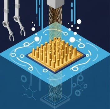
This is a continuous chemical reaction involving photolithography, electroplating, cleaning, stripping, and etching, known as the "wet process."
In this field, two companies in Taiwan have captured the absolute dividends from the global expansion of advanced packaging.
Honmax is the most critical and fiercely profitable equipment supplier in TSMC's CoWoS supply chain.
- 2026's "Sweet Trouble": Management revealed that current equipment order volumes already exceed their production capacity.
- Shipment Target: Plans to increase equipment shipments to over 220 units in 2026.
- Proactive Layout for 2028: Invested NT$1.1 billion to purchase 6,000 ping (approx. 1.98 hectares) of land in Hukou, Hsinchu, to build a new factory three times larger than its current scale.
- Targeting the Next Cycle: Not just for CoWoS, but for the CoPoS (Chip-on-Power-on-Substrate) wave beginning in 2028.
- Moat Data: Due to their extremely high technical complexity, CoPoS equipment is expected to have an ASP (Average Selling Price) 50% to 100% higher than existing CoWoS equipment.
If Honmax is a refined assassin, then Scientech is a strategically broad heavy-armored division.
- Dual Penetration of Foundry and OSAT: Self-developed equipment simultaneously penetrates the supply chains of major customers like TSMC and global OSAT players (such as Amkor, ASE).
- Beneficiary of Order Spillover: With CoWoS capacity projected to exceed 120,000 wafers per month by 2026, Scientech has become the preferred equipment supplier for orders spilling over to OSATs.
- Aggressive Expansion Plan: New factories in Hukou and Tainan are scheduled to be completed sequentially by the end of 2026 and 2027, aiming to boost equipment capacity to 2.5 times current levels by 2028.
- Reclaimed Wafer's Profitability Bulwark: Also has a reclaimed wafer business with a global market share of approximately 20%, serving as a stable defense line for operations.
💡 Strategic Conclusion: Who Cares About the Doctors? We Only Care Who Sells the Scalpels!
Through the analysis of these two "arsenal suppliers," we can draw an extremely sharp investment conclusion:
While the market is concerned about whether TSMC's CoWoS yield rate reaches 95%, the smartest capital is actually looking at Honmax and Scientech. Because as long as TSMC and ASE frantically expand production to catch up with NVIDIA's orders, they must dutifully place orders for machines from these two "wet process masters."
Moreover, this equipment demand is not a one-off. With the advent of the CoPoS era in 2028, the upgrade of equipment specifications will drive ASPs to new heights.
🏁 The Ultimate Esoteric Meaning: The Microscopic War Against Physical Distance
After reviewing the Bumping process and equipment supply chain, many investors might have a question: Why do we go to such great lengths, investing billions of dollars in R&D and capacity, just to grow those tens of micrometers of bumps on a chip?
Hidden behind this is a cold, hard truth that determines the value of computing power in the AI era: In the microscopic world of electronics, distance is the original sin.
General科普 articles will tell you that Bumping is to connect the chip to the substrate. But this is only half true.
If it were merely for connectivity, traditional wire bonding could also achieve this, and at a much lower cost. The true purpose of growing bumps is to "extremely shorten the distance."
Imagine that the gold wires of traditional wire bonding are like a winding mountain road, which must curve greatly from the chip's edge, extending several millimeters (mm), to connect to the motherboard.
For slow signals, these few millimeters are not a big deal; but for high-frequency AI signals flipping hundreds of billions of times per second (112G and above), these few millimeters of distance are a disaster.
These few millimeters of "mountain road" would generate severe parasitic inductance and capacitance (LC effect), making signals blurry, sluggish, and even generating massive amounts of heat.
Bumping, on the other hand, completely demolishes this mountain road, directly establishing tens of thousands of "high-speed express elevators" between the chip and the substrate, each only tens of micrometers long.
This is why the expansion pace of the equipment manufacturers we mentioned earlier (such as Honmax and Scientech) before 2028 is so crucial.
Because as processes evolve, our tolerance for distance has approached zero.
Performance Multiplier: According to industry data, evolving from the mature N28 process to the leading A16 process, the computing power improvement brought solely by process miniaturization is approximately 80 times; however, if coupled with advanced packaging technology that minimizes distance, the overall computing power improvement will leap to an astonishing 320 times.
This 4x performance gap is entirely hidden in those tens of micrometers of distance where the chip communicates with the outside world.
To extract every last bit of physical proximity, the entire semiconductor industry is moving towards even more audacious goals:
- CoWoS Revolution: Through Bumping technology, GPUs and HBM are placed so close that signal latency approaches zero.
- CoPoS (2028 Vision): This is the next wave we see in institutional reports — Chip-on-Power-on-Substrate. The future trend is that even "power supply units" will be directly attached to the bottom of the chip using ultra-complex Bumping technology.
- This will further eliminate voltage drop and losses during power delivery, allowing AI chips to withstand more extreme current loads.
This also explains why leading companies capable of handling such high-complexity, high-ASP equipment possess long-term appeal in the capital market's eyes.
🔄 Prelude to Spatial Flip: The Chip Is Ready to "Lie Down"
Now, let's connect all the dots.
Through 5-1-3, we confirmed the perfect soul of the chip; through 5-1-4, we outfitted it with powerful copper pillar boots.
But at this point, this chip is still "connected as one" with hundreds of its brethren, crowded on the same 12-inch wafer platform.
Before performing that "face down" spatial flip that completely revolutionized packaging history, we must first complete one of the most bloody and precise microscopic surgeries: limb separation.
Next, we will witness a yield defense battle evolving from "diamond blades traveling hundreds of kilometers per hour" to "silent lasers penetrating silicon wafers." Welcome to the extreme frontier of physical dicing.
In-depth Research · Quantitative Perspective
Want more insights into semiconductor quantitative research?
【Insight Subscription Plan】Break Free from Retail Investor Mindset: Build Your Alpha Trading System with "Quantitative Chips" and "Consensus Data"EDGE Semiconductor Research
📍 Series Map — Navigate the Complete EDGE Semiconductor Research →


