When we talk about semiconductor manufacturing, the media always loves to focus on ASML's hundreds-of-millions-of-dollars lithography machines. But for packaging plant managers, what often keeps them awake at night, or even directly leads to the instant scrapping of tens of thousands of dollars worth of AI chips, is often the last and seemingly crudest process: dicing.
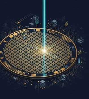
This is a 'surgical separation' performed under a microscope. On a 12-inch wafer, hundreds of completed high-end CPUs or GPUs are tightly connected. To place them into their respective packaging enclosures, we must use extremely forceful physical methods to cut them apart along the 'scriber lines' – paths only tens of micrometers wide between the chips.
🍪 The Lament of the Soda Cracker: The Fatal Allure of Low-k Materials
Why does this simple cutting action become a nightmare in advanced processes?
In 5-1-1, we mentioned a crucial keyword: Low-k (low-dielectric-constant materials). To achieve extreme computing power and low power consumption, the insulating layers of interconnects inside 3nm or 5nm chips use Low-k materials, which have an extremely loose structure. Physically, Low-k has only one characteristic: brittleness.
How brittle is it? It's like a soda cracker, less than a millimeter thick, fresh out of the oven.
When we use traditional 'blade dicing,' the blade, embedded with industrial diamond particles and approximately 20 micrometers thick, rotates at a terrifying speed of 30,000 revolutions per minute (rpm), leading high-pressure cooling water as it aggressively cuts into this soda cracker.
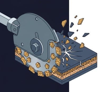
Imagine what happens when a diamond blade, moving at hundreds of kilometers per hour, cuts a soda cracker? Physical stress will wildly propagate along the cut surface. Under a microscope, you would see large areas of 'chipping' appearing at the chip's edges. What's even more terrifying is that the Low-k dielectric layer, unable to withstand the intense mechanical vibration, will experience internal 'delamination'.
A $500 3nm bare die could be instantly rendered dead if an extra micrometer of vibration during blade dicing causes a crack at the edge to extend into the circuit area. On a 12-inch wafer, this represents a yield catastrophe costing tens of thousands of dollars.
⚡ The Dead End of Mechanical Dicing: Cutting Too Fast Leads to Chipping, Too Slow to Low Throughput
Engineers at the traditional dominant player, Japan's DISCO (6146.T), once attempted to salvage mechanical dicing by improving blade materials and precise temperature control. But they quickly hit a physical wall:
- Blade Thickness Limitations: There's a limit to how thin a blade can be (approximately 15-20 micrometers). To accommodate the blade, the scriber line must be wide enough. But for 3nm processes, every micrometer increase in scriber line width means a reduction in the number of chips that can be produced on the entire wafer, directly impacting gross margins.
- Wafer Thinning Challenges: For HBM3e or ultra-thin mobile chips, wafers must be thinned from their original 775 micrometers down to just 50 to 100 micrometers (thinner than a sheet of copy paper). Such delicate, paper-thin wafers, when struck by a 30,000-rpm blade, would vibrate wildly like falling leaves in the water flow, making it impossible to maintain precision.
This is an unsolvable equation: cut too fast, and yield collapses (chipping); cut too slow, and throughput targets are missed.
🔦 The Dawn of Salvation: Micro-Ablation with Light
Just as mechanical dicing was about to become a critical drag on advanced processes, laser technology emerged as the sole savior.
However, the laser dicing discussed here is not like in Star Wars, where chips are burned through from the front. Burning would generate a significant amount of debris and a high-temperature 'Heat Affected Zone,' which would be equally fatal to wafers densely packed with nanoscale circuits.
To handle delicate Low-k materials, resembling fragile crackers, humanity developed a nearly sci-fi black technology – Stealth Dicing.
This technological revolution is poised to tear open a crack in the dicing market, which was originally monopolized by Japanese giant DISCO. And the report you provided indicates that the Taiwanese dark horse, Adoray (8027), is making a strong entry into this 'micro-ablation with light' battlefield, leveraging its deep understanding of laser applications.
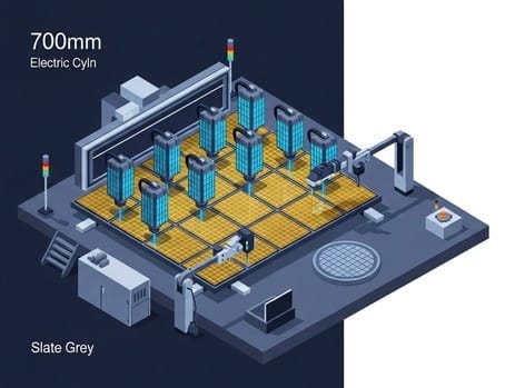
According to the latest institutional research report, Adoray not only has order visibility extending to Q3 2026 but has also successfully mastered key cutting and plasma etching technologies for FOPLP (Fan-Out Panel Level Packaging). Facing the demand for dicing massive 700mm*700mm panels, Adoray is employing a dual offensive of laser and plasma to provide certified equipment for advanced processes to major US semiconductor manufacturers.
The power shift on the dicing floor has only just begun. In the next section, I will explain how this 'silent, heatless, debris-free' Stealth Dicing works and why it turns an unassuming consumable like tape into a gross margin explosive.
🔦 Micro-Ablation with Light: From "Brute Force Destruction" to "Molecular Modification"
Traditionally, laser cutting is understood as using a high-energy beam to 'burn through' materials. However, when dealing with wafers in advanced processes, this approach is akin to using a flamethrower to cut whipped cream – the heat-affected zone (HAZ) generated by high temperatures would directly melt the delicate 3nm logic circuits.
Thus, a nearly sci-fi technology was born: Stealth Dicing.
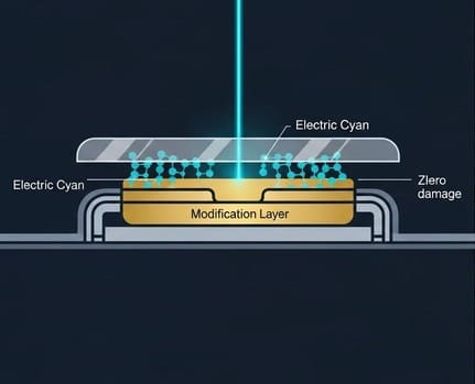
The logic behind this technology completely overturns thousands of years of human cutting experience: it doesn't operate from the surface; instead, it 'operates' from within the chip's 'belly.'
- Subsurface Stealth Penetration: Engineers adjust the laser's wavelength to make it 'transparent' to the silicon wafer. This laser beam passes unhindered through the precise nanoscale circuits (transistor and interconnect layers) on the wafer's surface, generating no heat.
- Precise Internal Blasting: The energy is precisely focused at the exact center of the wafer's thickness. At that instant, extremely high-density photons break the bonds of silicon atoms, forming an extremely thin 'modification layer' inside the wafer.
- Silent Separation: At this point, from the outside, the wafer still appears as a single, intact piece. However, internally, an 'artificial crack' has formed along the scriber line.
- Expansion and Fracture: Finally, through mechanical expansion using the underlying dicing tape, the wafer precisely and cleanly splits along this internal weakened line, much like tearing a postage stamp.
This revolution brings three overwhelming advantages: water-free (dry process), debris-free (prevents short circuits), and perfect 'zero chipping.' This allows the yield of wafers below 5nm, especially those with Low-k materials, to recover directly from the disaster zone of mechanical dicing to an ideal state of nearly 100%.
🧪 The Gross Margin Goldmine in Tape: The Consumable Legend of Dicing Tape
Do not underestimate the thin layer of 'tape' beneath the dicing machine. In the Stealth Dicing process, the tape is no longer just a mere holding medium; it is crucial for completing the dicing.
After laser modification, the wafer relies on this tape for 360-degree uniform stretching to separate the chips. This tape must possess extremely contradictory properties:
- Before Dicing: Extremely strong adhesion, must firmly grip the wafer, valued at tens of thousands of dollars, to prevent any displacement.
- After Dicing: Upon exposure to UV light (ultraviolet), the adhesion must disappear within one second, allowing the chips to be easily picked up by a suction nozzle.
This polymer material, known as UV dicing tape, is currently an absolute monopoly held by Japan's Nitto Denko and Lintec. In Taiwan, these high-gross-margin consumables are typically controlled by distributors with strong agency networks, such as Wah Lee (3010) or Chang Wah (8070), becoming another discreet cash cow for them alongside packaging materials.
🚀 The Dimensionality Reduction Strike by Taiwan's Dark Horse: Adoray (8027)'s Advanced Packaging Landscape
In this dicing battlefield, originally dominated by Japan's DISCO, Taiwan's Adoray (8027) is emerging as a dark horse with a completely different approach. According to the latest industry research, Adoray is no longer just a supporting player in laser printing; it has become an integrated 'light and chemistry' arms dealer in advanced packaging.
1. A Dimensionality Reduction Strike from WAFER to FOPLP Adoray's core growth driver comes from FOPLP (Fan-Out Panel Level Packaging). As NVIDIA and its US clients, in pursuit of higher area utilization, shifted packaging platforms from 12-inch circular wafers to massive 700mm*700mm square panels, traditional circular dicing machines faced a deadlock. Adoray, with its large panel laser dicing equipment, successfully secured positions with HPC (High-Performance Computing) and low-earth orbit satellite clients.
2. Profit Leap Rehearsal for 2026 Industry surveys indicate that Adoray's current order visibility extends clearly to Q3 2026. This is backed not only by dicing but also by Plasma Cleaning and Plasma Etching (Descum) equipment. After Stealth Dicing, chip edges often require plasma etching to remove microscopic residues. Adoray, through its integrated 'laser + plasma' solution, has successfully passed advanced process certifications from major US semiconductor manufacturers.
3. Violent Revenue Inflection Point Data from late 2025 shows Adoray's monthly revenue surged to NT$419 million (up 134% MoM, 146% YoY), reflecting that its advanced packaging equipment is entering a period of high-density certification and revenue recognition. Although short-term monthly revenue may fluctuate due to equipment delivery and accounting schedules, the market generally expects its revenue and EPS to grow exponentially in 2026 to 2027 as advanced packaging capacity comes online.
💡 Strategic Conclusion: Dicing, the Final Ritual for "Space Inversion"
Through this analysis of Stealth Dicing and Taiwanese equipment manufacturers, we can observe: dicing has evolved from a simple mechanical process into a complex battle involving 'optoelectronics + chemistry + polymer materials.'
Only when these excellent chips, 'wearing copper pillar power boots,' silently complete their 'surgical separation' via laser, do they qualify for independent operation.
Now, the chips are diced, and their 'shoes' are on. But not all chips are qualified to enter the tens-of-thousands-of-dollars AI battlefield. Before venturing into sophisticated Flip Chip packaging, we must first visit the 'undying veterans' who have toiled in the semiconductor industry for decades.
These veterans, though inexpensive, are the absolute backbone supporting global automotive, MCU, and power management chips. It was precisely the 'physical limits' of these veterans that compelled the subsequent space inversion revolution that shook the world.
In-Depth Research · Quantitative Perspective
Want more insights into quantitative semiconductor research?
【Insight Subscription Plan】Say Goodbye to Retail Investor Mindset: Build Your Alpha Trading System with 'Quantitative Capital Flows' and 'Consensus Data'EDGE Semiconductor Research
📍 Series Map — Navigate the Complete EDGE Semiconductor Research →


