Reading Tip: This article first uses "lead frame packaging" as a comparison to explain its long-term mainstream status in the world of hundreds of billions of chips, and breaks down the division of labor and moats of Taiwan's "Big Three" lead frame manufacturers. Finally, it returns to physical limits and connects to the inevitability of Flip Chip.
70%–80% of Chips Still Reside on Lead Frames
While all market attention is focused on TSMC's CoWoS advanced packaging and debates surrounding HBM stacking layers, one fact is often overlooked by investors: of the hundreds of billions of chips produced globally each year, over 70% to 80% still spend their entire lifecycle on traditional "lead frames."
If advanced packaging is the luxurious observation deck at the top of a skyscraper, then lead frame packaging is the "concrete and rebar" that supports the building, buried deep underground. Without it, our phones couldn't charge, our cars wouldn't start, and our home air conditioners wouldn't turn on.
🏗️ The Concrete and Rebar of Semiconductors: The Terrifying Economics of Lead Frames
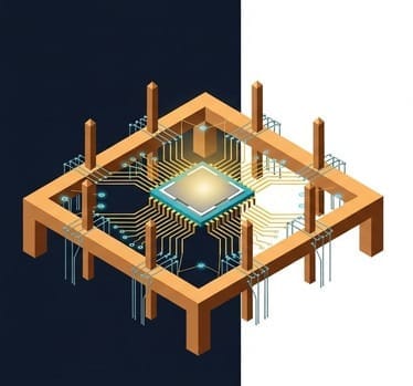
What is a Lead Frame?
What is a lead frame? Simply put, it's a thin copper sheet that has been precisely stamped or etched. The chip (die) is attached to its center, and then tiny gold or copper wires are used to connect the chip's signals to the external pins of the lead frame.
Underlying Logic: Geoeconomics × Material Management
The underlying logic of this business has nothing to do with cutting-edge technology; it's an extreme exercise in "geoeconomics" and "material management":
- Extremely Affordable Pricing: Packaging an advanced AI chip can cost hundreds of US dollars, but packaging a lead frame-based microcontroller (MCU) or power management IC might only cost 0.5 US cents. This terrifying scale economy makes it impossible for new entrants to compete on cost with established major manufacturers.
- A Fortress of Physical Resilience: While advanced packaging excels in controlled environments like AI data centers, lead frames demonstrate unparalleled thermal stability and mechanical strength under harsh conditions, such as under a car's hood or in high-temperature, high-vibration factory settings.
- Geographically Coupled Capacity Relocation: Lead frame manufacturers must operate in close proximity to outsourced semiconductor assembly and test (OSAT) companies and integrated device manufacturers (IDMs). As global IDM giants relocate production capacity to Southeast Asia (Malaysia, Vietnam) to mitigate geopolitical risks, Taiwan's lead frame manufacturers, leveraging decades of established collaboration, have become the most stable, invisible connectors in this wave of supply chain restructuring.
⚔️ Guardians of the Fortress: The Strategic Landscape of Taiwan's "Big Three" Lead Frame Manufacturers
In the seemingly traditional lead frame sector, three companies in Taiwan have carved out the most crucial global production capacity through exquisite craftsmanship and precise strategic acquisitions. Instead of competing fiercely with each other, they each dominate different lucrative segments.
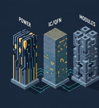
🏆 Shuen De Industrial (2351): The "Power Overlord" Master of Metallurgical Formulas
The story of Shuen De Industrial is a classic example of corporate transformation and upgrading in Taiwan. Starting as an office stationery manufacturer in 1967, it introduced Japan's Mitsubishi Shindoh as a strategic partner in 2010, directly acquiring technology licenses for special copper alloy materials for semiconductors. This "metallurgical DNA" has given Shuen De a near monopoly in the high-power semiconductor component sector. For electric vehicle manufacturers, in-car motor controllers must withstand immense current and waste heat, and only Shuen De's specially formulated lead frames can guarantee they won't burn out during high-speed operation. Shuen De is deeply integrated with global IDM giants like Infineon, STM, and ON Semi. More importantly, Shuen De holds low-cost copper inventory, and combined with an anticipated increase in processing fees in 2026, its gross profit margin is entering a period of significant expansion.
🏆 Chang Wah Technology (6548): The "IC Specification Definer" Born from Acquisitions
If Shuen De rose through in-house metallurgical research, Chang Wah Technology ascended to global leadership through precise "strategic acquisitions." In 2018, Chang Wah Technology boldly acquired the lead frame business unit of Japan's Sumitomo Metal Mining, directly inheriting advanced Japanese etching technology and global market share. Instead of directly competing with Shuen De in power components, Chang Wah Technology focuses on IC lead frames and QFN (Quad Flat No-leads) packages. QFNs are compact and dissipate heat quickly, making them the preferred choice for 3C products and 5G networking equipment. Anticipating the recovery of WiFi 7 and consumer electronics in 2026, Chang Wah Technology plans to significantly expand its QFN production capacity in China and Taiwan by 50% in the second half of 2026, and has successfully passed on rising raw material costs (such as gold, silver, and copper) to customers, demonstrating strong pricing power.
🏆 Jielin Technology (5285): The "Modular Pioneer" Deeply Rooted with Japanese IDMs
Compared to the prominence of the first two, Jielin Technology is a low-key yet extremely stable third player. Jielin's strategy also stems from acquisitions—it acquired another part of Sumitomo Metal Mining's portfolio (SHM Power Lead Frame). Jielin's moat lies in "power modules (IPM/PIM)." It doesn't just produce lead frames for single chips; it specializes in designing complex module frames that "bundle several power chips together" for Japanese and European IDM manufacturers. From inverter air conditioners to hybrid electric vehicles, Jielin has forged extremely deep ties with Japanese clients (such as Mitsubishi Electric and Rohm Semiconductor).
📈 Strategic Conclusion: Though Rough, Concrete Determines a Structure's Height
These "Big Three" lead frame manufacturers in Taiwan perfectly exemplify the phrase "quietly making a fortune away from the spotlight."
They are at the forefront of supply chain de-risking under geopolitical pressures (e.g., Chang Wah Technology receiving overflow orders from IDMs in Malaysia); moreover, they are among the few strongholds capable of expanding gross margins through raw material price increases amidst inflation.
However, while we marvel at the vitality of these veteran technologies, the shadow of physics still looms over them. As chips shrink to the size of a fingernail yet require thousands of interfaces to communicate with the outside world, the lead frame's logic of "arranging all metal wires along the chip's edge" has officially hit a physical limit.
🏗️ The First Hurdle: Die Bonding – The Life-and-Death Trade-off Between Silver Paste and Film
Securely attaching an extremely fragile bare die to a copper lead frame is certainly not as simple as applying a drop of superglue. Chips generate high temperatures during operation, and different materials have varying coefficients of thermal expansion (CTE). If not properly bonded, the chip could either overheat and burn out or be torn apart by thermal expansion and contraction.
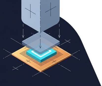
In the die bonding process, engineers face two distinct technological approaches:
- Conductive Silver Paste: The Robust Heat Dissipation Master
For most power components or automotive chips, engineers apply a blob of epoxy resin mixed with silver particles (silver paste) onto the lead frame, much like squeezing toothpaste. Its advantages are excellent thermal and electrical conductivity, and low cost. However, it has one fatal flaw: "bleeding." When the machine presses the chip down, the silver paste squeezes out from the sides. If chips are placed too close together, the extruded silver paste can cause a short circuit.
- Die Attach Film (DAF): The Double-Sided Tape for Extreme Stacking
When our mobile phones require stacking 8 or even 16 layers of NAND Flash memory chips (3D wire bonding stack), any bleeding of adhesive is absolutely unacceptable. This is where major chemical manufacturers invented DAF. It's a special "double-sided tape" dozens of times thinner than a human hair, pre-applied to the back of the wafer before dicing. After cutting, each chip comes with its own adhesive, which instantly cures upon heating and pressure. Although DAF offers poorer heat dissipation and is extremely expensive, it is the irreplaceable sole solution for ultra-thin stacked packaging.
🧵 The Second Hurdle: Wire Bonding – The Frenetic Microscopic Sewing Machine
Once the chip is secured, the truly breathtaking "microscopic embroidery" begins. The aluminum pads on the chip must be connected to the lead frame's pins, and this process is called Wire Bonding.
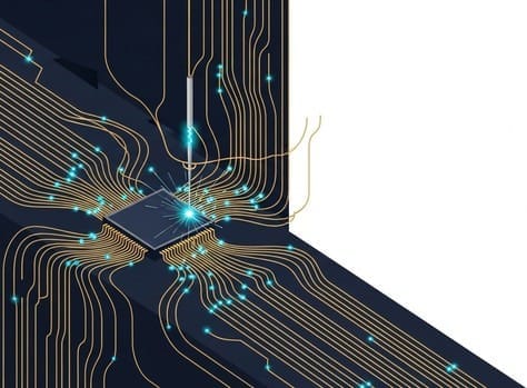
If you ever get the chance to step into a wire bonding cleanroom at ASE or ChipMOS, you'll see rows of machines emitting high-frequency buzzing sounds. Behind this hum lies the ultimate display of human mechanical engineering:
- Invisible Fineness: The metal wire used for bonding typically has a diameter of just 15 to 20 micrometers ($mu m$), roughly one-third to one-quarter the thickness of a human hair.
- Terrifying Speed of 15 Stitches Per Second: The "capillary" of a wire bonding machine acts like the needle of a microscopic sewing machine, guiding this incredibly fine metal wire as it frenetically moves between the chip and the lead frame. It must precisely "weld" the metal wire onto aluminum pads, which are only tens of micrometers wide, using ultrasonic vibrations and pressure under high temperatures.
- Extreme Specifications: A top-tier wire bonding machine can weld at an astonishing speed of 15 to 20 wires per second, with a placement accuracy error of no more than 3 micrometers for each wire! If even one wire is misaligned or if its loop is too high and touches an adjacent wire, the chip is immediately rendered scrap.
Invisible Equipment Giants
In the realm of wire bonders, the world is almost entirely monopolized by two companies: K&S (Kulicke & Soffa), headquartered in the United States, and Hong Kong-listed ASMPT (0522.HK). These two companies control the choke points for traditional outsourced semiconductor assembly and test (OSAT) manufacturers globally; any demand for wire bonding packaging necessitates paying equipment tolls to them.
⚔️ The Ruthless Material War: From "Gold" to "Common Metals" – A Compromise
In the past, wire bonding exclusively used pure gold wire. Gold was preferred because of its excellent ductility, resistance to oxidation, and the beautiful wire loops it produced.
However, under the brutal cost compression in consumer electronics, soaring gold prices became unbearable for packaging manufacturers. Consequently, packaging companies were forced to launch a breathtaking "material replacement war":
- The Rise and Cost of Copper Wire: To save money, manufacturers began switching to copper wire (which costs only a tenth of gold wire). However, copper wire has two fatal drawbacks: first, it oxidizes very easily, so during bonding, machines must continuously spray expensive forming gas (a nitrogen-hydrogen mixture) for protection; second, copper is very hard. When the capillary forcefully strikes the chip's aluminum pad with a copper wire, it can easily shatter the fragile underlying Low-k dielectric layer (the "soda cracker" we mentioned in 5-1-5), leading to a "cratering" effect.
- The Compromise of Palladium-Coated Copper and Silver Wire: To overcome the issues of pure copper's hardness and oxidation, material suppliers developed "palladium-coated copper wire (PdCu)," which has a surface layer of palladium, and "silver alloy wire," which offers high conductivity and is softer than copper.
This is an endless tug-of-war between cost and physics. Engineers are exhausting every ounce of their ingenuity, just to make a 0.5-cent package another 0.01 cents cheaper.
🧱 The End of the Physical Wall: Why Must These Veteran Technologies Stop Here?
Wire bonding packaging reaches its limits not because engineers aren't working hard enough, but because its inherent physical architecture presents two intractable fatal flaws in the face of the "computational power explosion" demanded by AI chips.
1. The Geometrical Death Sentence: The Perimeter Limitation Paradox
Wire bonding packaging operates under an ironclad rule: all signal connection points (pads) must be arranged along the "edge" of the chip. Imagine a chip as a bustling city; the logic of wire bonding is to cram all highway entrances to the outside world onto the city's "walls."
For a power management IC that only requires 50 pins, the "wall" space is more than ample. But what about NVIDIA's high-end GPUs? They require as many as 5,000 to 10,000 I/O (input/output) connection points! If all 10,000 of these connections had to be arranged along the chip's edge, the only way would be to infinitely enlarge the chip's area. However, in TSMC's 3nm process, every square millimeter of silicon wafer is incredibly valuable; making an expensive chip larger solely "to free up edge space for wire bonding" is absolute financial suicide. The perimeter simply cannot accommodate any more wires.
2. The High-Frequency Electromagnetics Disaster: Gold Wires Become "Broadcast Antennas"
Even if we manage to bond the wires, a second problem immediately emerges. As we mentioned in Article 5-1-3 on testing, AI chips transmit signals at speeds up to 112G PAM4. At such extremely high frequencies, a wire bond's gold wire, which is 3 to 5 millimeters (mm) long, physically ceases to be a mere conductor; it instantly transforms into a "transmitting antenna"!
When high-frequency signals pass through this long gold wire, severe parasitic inductance and capacitance (LC effects) are generated. Not only does the signal experience delay, but it also radiates out, interfering with adjacent gold wires (cross-talk). A digital "0 and 1" signal that was clean when transmitted from the chip becomes a mass of static noise by the time it reaches the motherboard via the gold wire.
Insufficient geometric space, coupled with excessively long physical distances. This is the insurmountable physical wall that wire bonding packaging can never overcome.
🚪 The Perfect Transition: When the Perimeter is a Dead End, We Must "Flip the Space"
When one path reaches its end, the only way to break the deadlock is to completely overturn the rules of the game.
Since the chip's "perimeter" can no longer accommodate more connection points, why don't we uniformly distribute the connection points across the chip's vast "area array"? And since a 5-millimeter gold wire transforms into an interfering antenna, why don't we eliminate that wire entirely?
To achieve these two audacious goals simultaneously, we must connect all the technologies learned in previous chapters: we no longer use gold wires. We utilize the technology prepared in Article 5-1-4 to uniformly grow tens of thousands of tiny "copper pillar bumps (Cu Pillar Bump)" across the chip's area. Then, we perform the greatest physical action in semiconductor packaging history—
We "flip" the chip directly. Face down, we press the bumps on the chip directly and firmly onto the contacts of the substrate!
No wires, no detours, no perimeter limitations. The distance between the chip and the substrate is instantly and drastically compressed from 5 millimeters to less than 0.1 millimeters.
This is Flip Chip packaging. It was not born to reduce costs; it is the ultimate form designed to unleash computational performance.
In-Depth Research · Quantitative Perspective
Want more insights into semiconductor quantitative research?
【Insight Subscription Plan】Break Free from Retail Investor Mindset: Build Your Alpha Trading System with "Quantitative Chips" and "Consensus Data"EDGE Semiconductor Research
📍 Series Map — Navigate the Complete EDGE Semiconductor Research →


