In a nutshell: Flip Chip, by 'flipping the chip over' and 'RDL redistribution,' releases I/O from the edges to the entire surface area, leading to reduced latency, increased bandwidth, and improved thermal dissipation. The trade-off is warpage caused by CTE mismatch, making Underfill a critical material. Ultimately, everything hinges on the ABF substrate as the expensive foundation and the supply-demand cycle in 2026–2027.
0) Starting Point of the Problem: Why 'Face-Up Chip' Became a Performance Disaster?
For the first fifty years of semiconductor development, engineers always approached chips with a 'face-up' posture.
The chip (die) was placed face-up, squarely on a lead frame or substrate, and then connected to the outside world using fine metal wires (Wire Bond).
But when TSMC scaled transistors to 3nm, and when NVIDIA furiously demanded that a GPU process hundreds of gigabytes of data per second, this 'face-up' posture became a performance catastrophe.
As we mentioned in the previous section (5-1-6), wire bonding encountered the fatal 'edge crowding paradox' and the 'gold wire antenna effect'. To break through this physical barrier, engineers had to make a move that completely overturned human intuition—Space Inversion.
1) Urban Traffic Metaphor: Eliminating the Waste of 'Detours'
To help you instantly grasp the significance of this spatial reversal, let's use an ultimate 'urban traffic' metaphor.
Imagine the inside of a chip as an extremely prosperous 'super downtown' with billions of inhabitants (transistors). This downtown area generates massive amounts of goods (data) every second, which need to be transported to the outside world (motherboard and memory).
- Under the wire bonding architecture, this downtown area is not allowed to build any external exits within itself.
- All goods must first travel through congested urban roads to the 'edge (city wall)' of the city.
- Then, the trucks drive onto a narrow, elevated bridge (gold wire) several kilometers long, suspended in mid-air, finally reaching the outer transfer station (lead frame pins).
This long 'suburban detour' is the culprit behind signal latency and the biggest black hole for wasteful power consumption.
Faced with this breakdown, engineers came up with a crazy idea:
"Since it's too far to go around to the edge, why don't we directly excavate a highway that goes straight to the outside world from underneath 'every block in the city center'?"
This is the core essence of Flip Chip (Flip Chip Packaging).
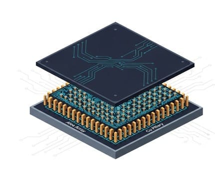
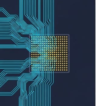
Engineers no longer cram the connection points (Pads) onto the chip's edges, but instead populate the chip's vast 'expanse (Area Array)' with thousands of tiny copper pillars (Cu Pillar Bump).
Then they performed that historic action: flipping the entire chip (Flip) over, face down, aligning thousands of copper pillars with the substrate contacts, and pressing it firmly down.
"Snap!"
There are no gold wires suspended in mid-air, nor any lengthy detours around the edges.
Every computational unit within the chip's downtown area, as soon as it 'steps out', can instantly reach the substrate below via the copper pillar beneath it, which is only tens of micrometers long.
2) But a Problem Arises: Contacts are Naturally on the Edges, How Do Copper Pillars Grow in the Main Area?
When chips are manufactured in a wafer fab, their inherent design still places 'contacts on the edges' (a legacy of decades). If it were simply flipped over, there would be no circuitry in the central area from which copper pillars could grow.
Therefore, before this magnificent 'flip' can occur, a massive 'underground subway paving project' must first be carried out on the chip's surface. This engineering feat will be the critical determinant of success or failure in advanced packaging.
3) Underground Subway System: The Magic of RDL (Redistribution Layer)
To uniformly distribute the highway entrances (contacts) originally crowded at the edges to the entire city center (chip's main area), we won't modify the expensive and complex transistor design within the chip.
We can only build an additional, entirely new transportation network on the chip's 'outermost layer':
RDL (Redistribution Layer).
You can imagine RDL as a 'microscopic underground subway system' built on the chip's surface. Engineers use photolithography and electroplating techniques to:
- First, lay a very thin insulating material (usually polyimide, PI) on the chip's surface.
- Then, 'draw' new metallic copper lines on the insulating film.
These microscopic copper lines have only one mission:
To horizontally extend and redistribute the contacts located at the chip's 'edges' to specified positions within the chip's 'main area'.
The contact distribution thus miraculously transforms from a crowded 'Peripheral' arrangement to a uniform 'Area Array'.
- Unlocking I/O Quantity Limitations: The edge length is limited, but the main area is vast. The number of I/O can surge from hundreds to thousands or even tens of thousands, becoming a physical prerequisite for the ultra-high bandwidth of AI chips.
- Distributing Stress, Preparing for Bump Growth: Only after contacts are uniformly distributed can 'copper pillars (Cu Pillar)' grow stably and uniformly support the structural stress after flipping.
Without RDL to pave the way, there is no place for copper pillars to stand; without copper pillars, Flip Chip's spatial reversal is merely empty talk.
Once this underground subway (RDL) is completed and tens of thousands of robust copper pillars are grown upon it, the chip is truly 'armed'—ready to 'lie face down'.
4) Compute Power Unleashed: The Three Major Performance Revolutions Brought by Flip Chip
When the gold wires of wire bonding are eliminated, and the chip is directly connected to the substrate 'face down', the computing system experiences three disruptive physical revolutions.
In traditional wire bonding, signals had to travel along gold wires up to 3–5 mm long.
Under the Flip Chip architecture, signals only need to pass through micro bumps less than 0.1 mm long, reducing the distance by approximately 50 times.
Parasitic capacitance and inductance (LC effects) are almost completely eliminated, signal latency approaches zero, enabling terabit-level data transmission between HBM and GPUs.
By using RDL to move contacts from the 'edges' to the 'main area (Area Array)', it's equivalent to transforming highway entrances from 'a ring around the city wall' to 'every street corner throughout the city center'.
The number of I/O (Input/Output) pins explodes from hundreds to thousands, or even tens of thousands.
In wire bonding, the chip faces up, covered with fragile gold wires, making it almost impossible to directly attach a heatsink.
In Flip Chip, the chip lies face down, with its flat, rigid, circuit-free pure silicon backside exposed upwards, allowing for direct application of thermal paste and attachment of a heat spreader and water cooling module.
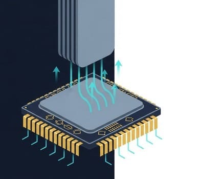
For AI behemoths whose power consumption easily exceeds a thousand watts, this is a matter of survival.
5) Physics' Cruel Bill: The Disaster of Warpage, Like a Curling Squid
Flip Chip appears to be flawless, but there's no free lunch in the physical world.
When a silicon die is soldered onto a plastic substrate via tens of thousands of copper pillars, it actually creates a dangerous 'thermodynamic bomb'.
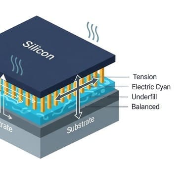
The Coefficient of Thermal Expansion (CTE) between silicon (chip) and plastic (substrate) is vastly different: plastic expands several times more than silicon when heated.
When an AI chip operates at full speed and its temperature rises above 80 degrees Celsius, the substrate aggressively stretches outwards while the silicon chip barely moves, creating immense tensile stress that causes the entire package to warp upwards (Warpage) like a squid on a grill.
This ultimately leads to solder joint cracks in the copper pillars in a very short time, rendering expensive modules scrap.
6) The Micro-Mason Saving Warpage: Underfill
To resolve this fatal cost, material chemists invented the indispensable life-saving elixir for advanced packaging:
Underfill.
The process is as follows:
- After the chip is flipped, pressed onto the substrate, and high-temperature soldering is completed
- A specialized epoxy resin is injected along the chip's edges
- Capillary action is used to fill the micrometer-sized gap between the chip and the substrate with the resin
- After baking and curing, it forms a rigid 'buffering compound'.
Underfill locks the chip, copper pillars, and substrate into a rigid integrated unit, absorbing and dispersing the tearing stresses caused by thermal expansion and contraction.
(Note: The chemical formulation battles of Underfill will be explored in greater depth in a future section, [5-2-7 Packaging Materials Chapter].)
7) Perfect Transition: Looking Down, at That Expensive 'Foundation'
The chip has been flipped, the copper pillars connected, and Underfill injected to lock everything in place. Performance is unleashed.
But don't forget: what exactly are the tens of thousands of precise copper pillars of this flipped chip resting upon?
The answer is a super-foundation whose circuit complexity approaches that of the semiconductor itself, and whose cost is extremely high:
ABF Substrate.
Without this substrate, Flip Chip would be an undecipherable book; without this substrate, NVIDIA's GPU would be nothing but a soulless silicon wafer.
8) The 'Super Foundation' Supporting Tens of Thousands of Copper Pillars: The Strategic Importance of ABF Substrates
After the chip is flipped face down, tens of thousands of copper pillars, spaced only tens of micrometers apart, must be precisely connected to a board.
This board cannot be a standard motherboard (PCB), as its traces are too thick and its holes too large to connect to microscopic copper pillars.
Therefore, a 'translator' must be inserted:
IC Substrate.
For AI and HPC chips pursuing ultimate performance, this translator must use top-tier ABF (Ajinomoto Build-up Film) material.
The complexity of ABF substrates is terrifying:
- To route the signals from tens of thousands of tiny contacts to larger solder balls at the bottom
- A top-tier AI ABF substrate may contain 16–20 layers of microscopic traces internally
- Each layer requires laser drilling, electroplating of blind vias, and precise alignment.
Any misplaced hole or shorted trace will render the substrate scrap.
Today, the manufacturing difficulty of high-end ABF substrates is no less than that of mature process wafer foundries; without ABF substrates, Flip Chip simply cannot be made.
9) The Golden Age of Substrate Giants: The Super Price-Hike Cycle of 2026–2027
Given the difficulty of creating such foundations, and the demand surging exponentially due to the increasing size of AI chips, a severe imbalance quickly emerged on the supply side.
According to our latest foreign institutional research (from BofA and HSBC), two major substrate giants in Taiwan are entering a sustained upcycle projected to last until 2027.
As a global ABF substrate leader, Unimicron's capacity is almost entirely taken up by NVIDIA, AMD, and Intel.
What excites the market even more is the 'Pricing Upside'.
Due to a severe shortage of the upstream core material, T-Glass (specialized glass fiber fabric), coupled with the recovery of AI and high-end server CPUs, ABF substrates have entered a seller's market.
Foreign institutions predict that the ASP for ABF and BT substrates from Taiwan's top three substrate manufacturers could increase by 23%–30% in 2026.
In manufacturing, if costs remain constant, this additional revenue from price increases can be highly converted into profit, which is why foreign institutional forecasts for Unimicron's earnings often lead market consensus.
If you find Unimicron too crowded, Nanya PCB is a turnaround stock with stronger explosive potential in this upcycle.
In the past two years, Nanya PCB was dragged down by inventory adjustments in consumer electronics, but a BofA report indicates it received a rare 'Double Upgrade to Buy'.
The engine driving Nanya PCB's takeoff is:
'Order spillover from AI ASICs (customized AI chips)'.
As cloud giants (such as Google, AWS, and Meta) accelerate their self-developed ASICs and reduce their reliance on NVIDIA, they also require large quantities of ABF substrates.
Once Unimicron's capacity is fully utilized, overflow orders are directed to Nanya PCB, boosting its capacity utilization and gross margins in 2026–2027, thus ushering its profits into an expansion phase.
10) Strategic Conclusion: Whoever Controls the Foundation Collects Rent from AI Giants
Through this entire section, 5-1-7, we have completed a convergence of 'technology → physical cost → industry implications'.
- Eliminating detours for downtown access: Flip Chip
- Underground subway on the chip surface: RDL
- The micro-mason against warpage: Underfill
- Finally landing on the 'foundation': ABF Substrate
This is no longer traditional 'packaging'.
This is an extreme spatial war waged to extract every last drop of computing power from chips.
And Unimicron and Nanya PCB are the most irreplaceable arsenals in this war.
Whoever controls substrate capacity has the right to collect the most expensive tolls from the world's top AI giants.
Deep Research · Quantitative Perspective
Want more insights from semiconductor quantitative research?
[Insight Subscription Plan] Bid Farewell to Retail Investor Thinking: Build Your Alpha Trading System with 'Quantitative Capital Flows' and 'Consensus Data'EDGE Semiconductor Research
📍 Series Map — Navigate the Complete EDGE Semiconductor Research →


