Subject: Moore's Law is reaching its limits in the 3nm/2nm era. The solution is to break down "large chips" into Chiplets and then reassemble them using advanced packaging.
For the past five decades, the approach to Moore's Law has been straightforward: making transistors smaller and smaller, and packing more and more functions into a single chip (SoC, System-on-Chip). CPUs, GPUs, memory controllers, and I/O interfaces were all integrated into one giant silicon chip.
However, in the 3nm and 2nm era, this "big package" aesthetic has officially hit two insurmountable physical and economic walls.
🧱 The First Wall: The Physical Death Sentence of the Reticle (Reticle Limit)
Why don't we just make a chip as large as a bento box? Because the creator (or rather, ASML) doesn't allow it.
In a wafer fab, the maximum area exposed by a lithography machine in a single pass is known as the "Reticle Limit." Currently, the most advanced ASML EUV exposure machines can print a maximum area of approximately 26 mm × 33 mm, which is 858 square millimeters.
- Physically, it's impossible to print a single chip larger than 858 square millimeters with one lithography machine.
- Today, NVIDIA's most advanced AI chips are already approaching this limit.
The growth of single chips has effectively been sentenced to death at this point.
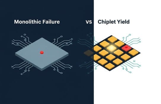
🎂 The Second Wall: The Cruel Yield Math of Baking Cakes
Even if the reticle limit could be overcome, economics would immediately stifle such a colossal chip. This involves the most brutal math in semiconductor manufacturing—the multiplicative effect of yield.
Imagine that manufacturing an ultra-large SoC chip is like baking a giant, premium 12-inch cake in an oven. During the months-long process involving thousands of chemical and physical steps:
- Even if an invisible speck of dust falls in the cleanroom
- Or a nanoscale exposure is slightly out of focus
A corner of this ultra-large cake will "burn."
In the world of traditional SoCs, if even one corner is burnt, the entire chip, costing tens of thousands of dollars, must be discarded completely.
The larger the chip area, the geometrically higher the probability of capturing dust (defects). For example:
- If a chip is divided into three blocks
- And each block has a 90% yield
Then the total yield for the entire large chip is a cruel multiplication: 0.9 × 0.9 × 0.9 = 0.72 (72%).
If the area is further enlarged, the yield would rapidly plummet towards zero. This rate of burning cash would bankrupt even Apple and NVIDIA.
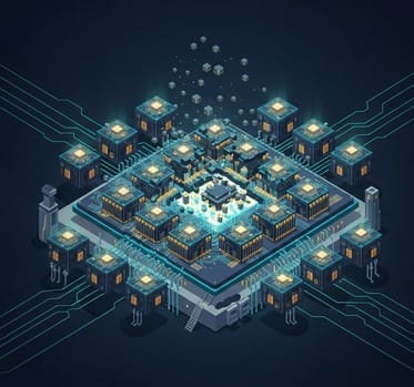
🪄 Chiplet's Desperate Survival: Turning "Multiplication" into "Addition"
Since making one ultra-large cake is prone to failure, brilliant engineers had a change of thought: Why don't we, from the start, cut the cake into individual "cupcakes," bake them, and then assemble them afterward?
This is the underlying logic behind the birth of Chiplet technology.
- We no longer insist on cramming all functions into a single 858 square millimeter behemoth.
- Instead, we "disassemble" it, cutting it into 10 smaller chips, each only 80 square millimeters.
Now, the magic of yield happens: with extremely small chiplet areas, yields can easily approach 99%.
- Even if one of the small chips "burns" during manufacturing
- We simply need to discard that faulty chiplet
- And replace it with a good one
The other 9 perfect chiplets remain completely unaffected.
By disassembling large chips into Chiplets, the yield calculation in wafer fabs instantly transforms from cruel and unforgiving "multiplication" into highly fault-tolerant "addition." We only pay for "truly perfect silicon," no longer footing the bill for collateral damage.
💰 Good Steel Used on the Blade: The "Cost Arbitrage" of Heterogeneous Integration
In the past SoC (System-on-Chip) era, the entire chip could only utilize "a single type" of manufacturing process.
- If the core logic computation requires the most cutting-edge and expensive TSMC 3nm process
- Then the SRAM (cache memory) or I/O (input/output transmission interface) packaged within the same chip
Could only reluctantly be printed using the 3nm process as well.
But this is an extremely foolish waste from an economic perspective.
- Because I/O interfaces simply don't require 3nm miniaturization; they can operate just as fast using 6nm or even 28nm processes
- And SRAM's scaling benefit at 3nm is extremely low; printing SRAM with a 3nm process is akin to making garbage bags out of Hermès leather
When Chiplet technology emerged, this long-standing pain point was instantly resolved. It introduced the most captivating concept in advanced packaging: Heterogeneous Integration.
Engineers can now perform extreme "cost arbitrage" as if playing with LEGO bricks:
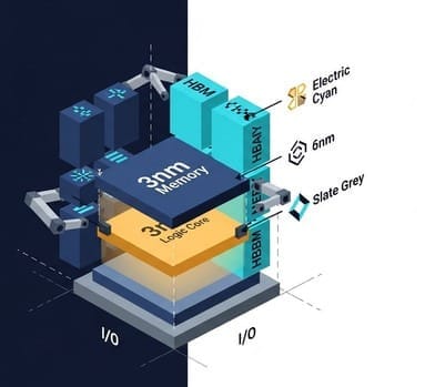
- Brain (core compute): Manufactured using the most expensive 3nm or 5nm process to extract maximum computing power.
- Limbs (I/O chiplets): Manufactured using cheaper 6nm or even mature processes.
- Memory (HBM): Purchased directly as pre-stacked chips from memory manufacturers (SK Hynix or Micron).
Finally, these chiplets, originating from different processes and different wafer fabs, are all assembled together using advanced packaging technologies (such as TSMC's CoWoS or SoIC). This not only significantly reduces development costs but also enables IC design companies to iterate products at the fastest possible speed.
🏎️ The AMD MI300 Counterattack: A Textbook Example of Chiplet's Brutalist Aesthetics
If there's one player who is the fiercest in this Chiplet cost and performance arbitrage game, it is undoubtedly AMD.
Facing NVIDIA's absolute dominance in the AI chip sector, AMD knew that a head-on confrontation with a conventional ultra-large SoC would leave them with no chance due to yield and cost issues. Thus, AMD unveiled the most audacious Chiplet assembly artistry in semiconductor history—the MI300 chip.
Take a closer look at the MI300's internal structure; it is an extreme example of micro-brutalist aesthetics:
- The Foundational Layer (I/O Chiplets): AMD first took 4 I/O and base compute chiplets manufactured using TSMC's 6nm process and laid them side-by-side on the interposer.
- The Top Layer of Compute (CPU/GPU Cores): Next, AMD introduced 9 core compute chiplets (including GPU and CPU cores) manufactured using TSMC's 5nm process.
- Seamless 3D Stacking (SoIC): Instead of arranging them flat, AMD utilized TSMC's most advanced 3D packaging technology (SoIC) to directly "stack" these 9 5nm compute chiplets on top of the 4 6nm I/O chiplets.
- The Surrounding Moat (HBM): Finally, 8 High Bandwidth Memory (HBM3) stacks were placed around these stacked chip towers.
Through this "chop and re-assemble in 3D" black technology, the AMD MI300 successfully packed an astonishing 153 billion transistors into a single package.
If these 153 billion transistors were to be strictly manufactured on a single 5nm chip:
- The reticle would not be able to print it
- And the yield would undoubtedly be a dismal 0%
Through Chiplet heterogeneous integration, AMD not only bypassed the reticle limit, achieving unimaginable compute density, but also executed a critical cost-based overtake against NVIDIA.
🗼 The Babel Tower of Communication: Chiplet's Fatal Flaw and the UCIe Standard
In the SoC (System-on-Chip) era, all transistors resided on the same piece of silicon, speaking a common language, with signal transmission distances of only a few micrometers.
However, upon entering the Chiplet era:
- Chip A might be a logic computation unit made by TSMC's 3nm process
- Chip B might be an I/O interface made by Samsung's 6nm process
- Chip C might be memory from SK Hynix
Forcibly combining them on the same interposer is like locking people who speak French, Japanese, and Arabic in the same room and forcing them to translate an entire encyclopedia in one second.
This is the "Babel Tower Crisis" in the semiconductor industry. Without a unified language and ultra-fast bridges, the enormous power consumption and latency generated by Die-to-Die (D2D) transmission would completely negate all the cost advantages brought by heterogeneous integration.
To resolve this crisis, in 2022, global giants such as Intel, AMD, TSMC, and ASE jointly launched the ultimate standard poised to dominate the fate of packaging for the next decade—UCIe (Universal Chiplet Interconnect Express).
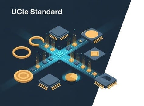
UCIe is like the "USB Type-C" of the chiplet world. It stipulates that all chiplets, regardless of their manufacturer, must adopt this unified physical layer and communication protocol.
As long as everyone speaks the UCIe language, future IC design companies can even "shop online" for off-the-shelf chiplets and then, like a puzzle, perfectly assemble a top-tier AI behemoth.
💰 The Ultimate Harvesters: The IP Duopoly and the Squared Bonus of Substrates
Understanding the importance of D2D transmission and UCIe allows us to accurately identify the invisible powerhouses in this Chiplet puzzle game who, without building factories or bearing depreciation, collect the most substantial "tolls."
The Profitable Harvest of Silicon IP: Alchip Technologies (3661) and Global Unichip (3443)
When global cloud giants (AWS, Google, Microsoft) seek to build their own AI ASICs (customized chips) using Chiplet architecture, they face a problem: they understand AI algorithms, but they have no idea how to design the extremely complex "D2D high-speed transmission interfaces."
- Both companies are deeply integrated with TSMC's advanced processes and advanced packaging (such as CoWoS's GLink IP)
- They hold the most advanced D2D transmission "blueprints (silicon IP)"
Whenever an IC design house wants to assemble two chiplets, it must purchase these blueprints from them. This is a highly lucrative business with extremely high gross margins (licensing fees are almost pure profit).
As long as the Chiplet trend continues, the more fragmented chiplets become, the greater the number of "communication bridges" required, and the more astonishing the royalties collected by these IP providers will be.
The Squared Bonus for Substrate Manufacturers: Unimicron Technology (3037) and Nanya PCB (8046)'s Underlying Frenzy
In 5-1-7, we discussed the 23% price surge storm in ABF substrates, and Chiplet is an even greater catalyst for this storm.
When chips are broken down into smaller pieces, and in pursuit of higher total computing power, engineers lay out 10 or even 20 chiplets flat on the same package substrate.
This has led to a monstrous expansion in the area of the ABF substrates that carry them:
- From the traditional 50×50 millimeters
- Surging to 100×100 millimeters or even larger
While the area doubles and yield drops exponentially, the ASP (Average Selling Price) of substrates skyrockets geometrically.
As long as the chiplet puzzle continues to expand, giants like Unimicron Technology and Nanya PCB, who control these "super foundations," will enjoy a squared bonus in this frenzy.
🚪 Perfect Transition: How to "Place the Puzzle Pieces Close Enough"?
In 5-1-8, we thoroughly deconstructed the disintegration and rebirth of Moore's Law.
Now, we have:
- Affordable and high-yield chiplets
- A unified communication language (UCIe)
- Design blueprints for transmission (IP vendors)
However, there remains one crucial physical challenge: for UCIe's high-speed transmission to be effective, the physical distance between these chiplets must be reduced to within "tens of micrometers."
If they are merely placed casually on an ABF substrate, the rough traces on the substrate simply cannot support such micrometer-scale dense interconnections.
We must insert an additional layer between the chiplets and the ABF substrate: an "ultramicroscopic glass bridge that is a hundred times more precise than the substrate, intricately sculpted with foundry-grade Extreme Ultraviolet (EUV) lithography."
This bridge is currently the most sacred and most expensive ultimate weapon in the semiconductor industry, and the one NVIDIA CEO Jensen Huang daily presses TSMC for production capacity.
The name of this weapon is CoWoS.
In-depth Research · Quantitative Perspective
Want to gain more insights into semiconductor quantitative research?
[Insight Subscription Plan] Bid Farewell to Retail Investor Mentality: Build Your Alpha Trading System with "Quantitative Chips" and "Consensus Data"EDGE Semiconductor Research
📍 Series Map — Navigate the Complete EDGE Semiconductor Research →


