Positioning: This section uses "2016 iPhone 7 / A10 + InFO" as a watershed moment to explain how TSMC entered back-end packaging from front-end manufacturing, and how it established a structural advantage over OSATs through process capabilities and co-design.
Foreword: The "Peace Treaty" Before 2016
Before 2016, an unspoken "peace treaty" existed in the global semiconductor industry: foundries stayed foundries, and OSATs stayed OSATs.
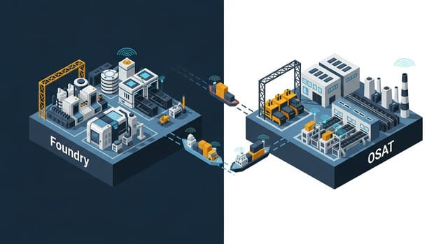
Foundries like TSMC and UMC were responsible for donning cleanroom suits and using expensive photolithography equipment to print transistors onto silicon wafers. After printing, the wafers would be packaged and sent out the door to professional Outsourced Semiconductor Assembly and Test (OSAT) companies, who would then perform dicing, wire bonding, or flip-chip packaging.
Everyone kept to their own lane, earning profits from different segments of the industry chain.
Until 2016, when Apple was preparing to launch the iPhone 7, this peace treaty was instantly torn up. The OSAT industry refers to this as the "Pearl Harbor incident" they will never forget.
⚡ The 2016 OSAT Earthquake: Apple A10 Chip's Exclusive Coup
At the time, orders for Apple's A-series processors had long been split between TSMC and Samsung of Korea.
However, with the iPhone 7's A10 processor, the market was alarmed to discover that TSMC not only completely edged Samsung out, gobbling up 100% of Apple's foundry orders, but it also did not hand over the wafers to external OSATs. Instead, TSMC handled the entire "manufacturing to packaging" process from start to finish within its own facilities.
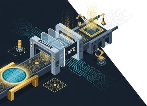
The ultimate weapon TSMC used to secure this historic mega-order was called InFO (Integrated Fan-Out).
📏 Extreme Slimming Technique: Removing the Bulky "Foundation" Directly
Why would Apple, for the sake of InFO, break its long-standing "diversified supplier" strategy and willingly entrust its lifeline entirely to TSMC? Because Apple has an almost obsessive demand for the iPhone: extreme thinness and lightness.
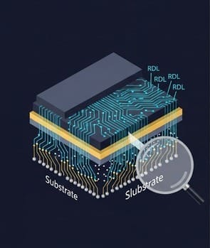
We discussed Flip Chip packaging in 5-1-7. While Flip Chip offers powerful performance, it comes with a critical spatial cost: it relies on a thick IC substrate as a foundation to route the chip's tiny signals to the phone's mainboard.
For the iPhone's internal space, where every millimeter counts and even 0.1mm is scrutinized, this substrate was simply "too thick and took up too much space."
Thus, TSMC's engineers proposed an idea that, at the time, seemed insane: "If the substrate is too thick, then let's just remove it!"
🧱 The Physical Essence of InFO: How to Fan-Out Signals Without a Substrate?
But without a substrate, how can chip connections fan out to the mainboard? InFO demonstrated an astonishing physical essence:
- Embedded in Artificial Amber: TSMC precisely arranged the diced裸晶 (bare dies) on a temporary carrier, then "poured and encapsulated" them all with black epoxy resin (Mold Compound), much like insects encased in artificial amber.
- Conjuring Shortcuts from Nothing: Once the amber hardened, TSMC directly utilized the high-precision photolithography equipment from its wafer fabs to precisely engrave the RDL (Redistribution Layer), which we discussed in the previous section, onto the flat surface of this "artificial amber and chip" composite.
- The Substrate-less Miracle: Through the RDL, the chip's signals fan out directly across the amber's surface, and finally, solder balls are attached.
Effect: Without a traditional substrate, the thickness of the entire package was instantly reduced by over 20%.
- Greatly improved heat dissipation efficiency
- Shorter signal paths, leading to faster transmission and lower loss
Upon seeing this technology, Apple immediately placed all its orders with TSMC. InFO not only made the iPhone 7 thinner and freed up more space for the battery, but it also formally declared the beginning of TSMC's packaging hegemony.
But why would TSMC go to such great lengths to encroach on the OSAT business? Was it merely to earn a little extra from packaging processing fees?
Absolutely not. Behind this lies a "dimension-reduction strike" and "ecosystem binding" business logic that left competitors in despair.
☄️ Dimension-Reduction Strike: When "Nanometer-Scale" Sniper Rifles Face "Micrometer-Scale" Flintlocks
In business strategy, a "dimension-reduction strike" refers to using weapons and thinking from a higher dimension to crush a lower-dimension opponent, leaving them no chance to retaliate. TSMC's entry into packaging is one of the most brutal dimension-reduction strikes in semiconductor history.
Traditional OSATs have long been accustomed to a "micrometer ($\mu m$)" level of warfare. Their equipment, cleanroom standards, and engineers' mindset are all built on the micrometer scale.
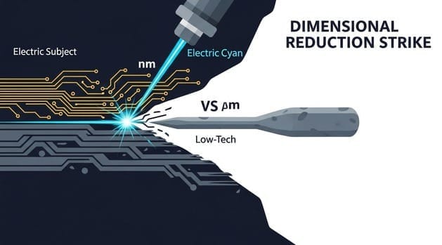
But who is TSMC? It's a champion forged in the hellish difficulty of the "nanometer (nm)" scale.
When TSMC decided to move its fully depreciated photolithography equipment, originally used to print 28nm or 45nm wafers, and deploy it for RDL (Redistribution Layer) engraving at the packaging level, a miracle happened.
The line width and spacing (L/S) limit for RDLs made by traditional OSATs using substrates is approximately 10 to 15 micrometers. But with TSMC's wafer-level equipment, simply by deploying it, the RDL line width was directly compressed to 2 micrometers or even lower.
This is like using a modern sniper rifle equipped with thermal imaging against a group of soldiers still loading gunpowder into flintlocks. Traditional OSATs, even if they spent everything they had, could not afford wafer fab-grade steppers to perform packaging.
TSMC didn't just seize business; it violently elevated the "precision ceiling" of packaging to a height that OSATs simply could not reach.
⛓️ Wielding the Emperor to Command the Dukes: The Ultimate Binding of Co-design
But this is not the most terrifying aspect. TSMC's underlying strategy for advanced packaging actually stems from a deep sense of "anxiety."
TSMC's calculation was:
"If I spend $20 billion building a 3nm wafer fab, and then the customer hands their 3nm chip to an external OSAT, only for the 3nm performance to be throttled because of poor heat dissipation or narrow I/O bandwidth from traditional packaging, then why would customers spend big money on my 3nm wafers in the future?"
To address this anxiety, TSMC had to personally break through the physical bottlenecks of packaging to ensure customers could experience 100% of the power of the most advanced processes.
Thus, TSMC presented an irresistible offer to top-tier customers like Apple and AMD: Co-design.
In the past, IC design companies would first complete the chip design, have it fabricated, and then figure out how to get it packaged by an OSAT.
However, in the Co-design model, the internal transistor architecture of the chip and the external InFO package (including RDL routing and heat dissipation structures) are "integrated and co-developed" from the very first day of design.
This resulted in an extremely brutal business consequence: Lock-in.
Once Apple's A-series processors were tailor-made for TSMC's InFO packaging, Apple could no longer switch orders to Samsung or Intel. Because with any change in foundry, the entire set of physical designs and thermodynamic models, from front-end to back-end, would become invalid, rendering the chip inoperable.
TSMC was no longer just selling "a silicon wafer full of transistors"; it was selling an inseparable computing system where "without me, your chip cannot breathe."
🌳 The Sprawling Packaging Empire: The Comprehensive Invasion of the InFO Family
TSMC's engineers have exquisitely fine-tuned the fundamental InFO architecture, giving rise to an "InFO family" that has suffocated traditional OSATs:
- InFO_PoP (Package on Package): This is the ultimate form tailor-made for smartphones (and Apple's preferred technology for iPhones). TSMC not only embeds the CPU/GPU at the bottom layer but also drills countless tiny "Through-InFO Vias (TIVs)" within the package, allowing third-party DRAM (memory) to "stack" directly on top of the processor, much like building a skyscraper. This drastically compresses the motherboard area in phones.
- InFO_oS (on Substrate): As this technology moved towards "networking chips" and "edge computing," TSMC integrated multiple chiplets with different functions using InFO technology, and then placed them on a larger, traditional substrate. This effectively captured business from high-end Flip Chip packaging.
- InFO_B (Bottom only, Cost-reduced Modularization): To address the issue of Android smartphone manufacturers finding InFO too expensive, TSMC introduced "InFO_B," which only processes the bottom half. TSMC handles the most complex logic processor packaging and RDL fabrication, then hands this "semi-finished product" to smartphone manufacturers, allowing them to find external OSATs to stack the memory themselves. This "flexible cost reduction" strategy directly ignited competition in the mid-to-high-end consumer market.
🏴☠️ A Declaration of the Era: The Complete Disappearance of the Front and Back-End Divide
Having reviewed the proliferation of InFO, we must now draw a historical strategic conclusion.
The battle of 2016 meant far more than "the iPhone getting thinner." It declared a cruel truth to the world: the boundary between "front-end manufacturing (wafer foundry)" and "back-end packaging (OSAT)" has officially vanished.
In the past, the semiconductor industry was like an assembly line, with everyone earning profits in their turn. But TSMC, with InFO, proved that as long as one mastered the most advanced photolithography and material chemistry technologies, wafer foundries could cross that line at any time and devour the juiciest back-end profits.
🚪 A Perfect Transition: OSAT Giants Awakened in the Dead of Night
As TSMC proudly showcased the astonishing revenue generated by InFO during its earnings calls, one can imagine the immense panic that permeated the headquarters of ASE (3711) in Kaohsiung, Taiwan, and the boardrooms of Amkor (AMKR) in the United States.
These traditional OSAT giants woke up in the dead of night. They looked at the equipment in their fabs, adept at wire bonding and traditional flip-chip packaging, and suddenly realized a chilling reality:
"If even packaging requires nanometer-scale wafer lithography equipment, what does the future hold for those of us without wafer fabs? Are we destined to merely pick up the low-margin assembly work that TSMC leaves behind?"
This is a life-or-death struggle for survival. Traditional OSATs have been pushed to the edge of a cliff; they have no retreat and are forced to choose "violent upgrade."
In-depth Research · Quantitative Perspective
Want to gain more insights into semiconductor quantitative research?
【Insight Subscription Plan】Break Free from Retail Investor Mindset: Build Your Alpha Trading System with "Quantitative Chips" and "Consensus Data"EDGE Semiconductor Research
📍 Series Map — Navigate the Complete EDGE Semiconductor Research →


