🧱 Fatal Physical Contradiction: When "Supercars" Drive on "Mudslide Industrial Roads"
To truly understand the greatness of CoWoS, we must first revisit the brutal reality faced by the "Chiplet (small chip) Lego Puzzle" mentioned in 5-1-8.
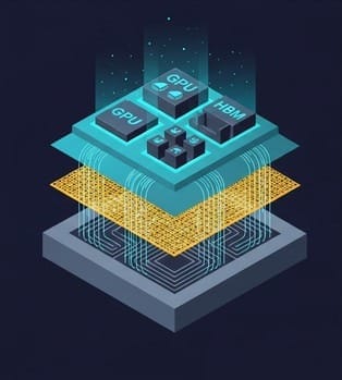
After engineers divide a massive AI chip into GPU chiplets for computation and HBM (High Bandwidth Memory) chiplets for memory, the next step is to place all these chiplets onto a "foundation" to enable them to connect and communicate.
As we discussed in 5-1-7, this foundation is called an ABF substrate.
In the past, placing chips on ABF substrates was perfectly reasonable. However, as we enter the era of AI, the data transfer volume between HBM memory and GPUs has reached astonishing astronomical figures of several terabytes (TB) per second. This implies that thousands of extremely fine physical metal lines are needed to connect these two chips.
At this point, a fatal physical contradiction emerged: a dimensional disparity in thickness.
NVIDIA's GPUs and HBMs are manufactured using TSMC's 5nm or 3nm processes, with internal circuits so fine they are measured in nanometers (one ten-thousandth the size of a red blood cell). However, the underlying ABF substrate is made of plastic material and copper foil, and even the world's leading substrate manufacturers (such as Unimicron and Nanya PCB) can only etch lines as fine as approximately 10 to 15 micrometers (µm) on plastic.
This is a thousand-fold difference!
Please imagine a vivid metaphor:
GPUs and HBMs are like two supercars capable of speeds up to 500 km/h, but the traces on the ABF substrate are like a bumpy, uneven rural dirt industrial road.
If you insist on placing these two chips flat on an ABF substrate and having them communicate via the coarse copper lines within the substrate, what would happen?
The supercar's speed would instantly drop to zero upon hitting the dirt road. When extremely fine signals enter the coarse substrate traces, they generate significant resistance and capacitance delay (RC Delay). The signals not only fail to transmit quickly but also produce extremely high heat and consume a large amount of power.
This is the biggest crisis in the history of AI chip development: no matter how powerful a chip's computing capability, if its foundation is too coarse, everything is in vain.
🌉 TSMC's Bridge-Building Magic: A "Microscopic Highway" Built from Pure Silicon
Facing this intractable physical deadlock, TSMC's engineers proposed a "bridge-building" concept that stunned the industry.
They thought to themselves: "Since the underlying ABF substrate is too coarse, why don't we create an 'extremely flat, extremely dense' interposer ourselves, to be placed between the chips and the substrate?"
This miraculous interposer is the soul of advanced packaging — the Silicon Interposer.
Why must this interposer be made of "Silicon"?
Because the surface of a silicon wafer, after polishing, is one of the flattest materials known to humankind. More importantly, TSMC possesses the world's most advanced photolithography equipment (steppers/scanners)! TSMC can directly use the machines employed for printing chips in its fabs to print ultra-high-density connections with line widths of less than 1 micrometer on this "pure silicon interposer".
Returning to the earlier metaphor:
With this silicon interposer, TSMC has essentially conjured an incredibly flat, multi-lane "exclusive elevated microscopic highway" above the rugged dirt road (ABF substrate).
Now, GPUs and HBMs only need to transmit data to each other on this pure silicon highway, with lightning speed, completely bypassing the coarse dirt road below. Only when this entire computing module needs to communicate with the outside world (e.g., motherboard, power supply) will signals be transmitted downwards through specific channels to the ABF substrate.
This microscopic highway completely unlocked the bandwidth barrier between HBM and GPUs and officially opened the door to Generative AI.
✂️ Decoding CoWoS: An Extremely Precise Surgical Operation
Having understood the existence of the "microscopic highway", we can now finally deconstruct the acronym that has captivated investors worldwide: CoWoS.
CoWoS is not a single technology; it describes a top-down, two-stage "three-dimensional assembly process". The full name is Chip-on-Wafer-on-Substrate.
Let's break it down:
- The Chip here refers to chiplets like GPUs and HBMs.
- The Wafer here refers to the aforementioned "microscopic highway built from pure silicon (silicon interposer)".
- Action: TSMC must use extremely precise machinery to accurately solder (micro-bump bonding) the GPUs and HBMs onto this pure silicon interposer.
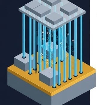
- Devil in the Details (TSV Through-Silicon Via): Since the silicon interposer is situated between the chips and the bottom substrate, how are the chips powered? TSMC must use lasers or chemical etching to create tens of thousands of extremely tiny vertical deep holes, drilled from top to bottom, through this delicate pure silicon highway, and fill these holes with copper. This is known as TSV (Through-Silicon Via), akin to drilling countless elevator shafts through an elevated highway directly to the ground, allowing current to be supplied directly upwards to the GPU from the lowest substrate. This step is extremely difficult, and yield control is exceptionally challenging.
- The Substrate here is the familiar ABF plastic substrate (dirt road).
- Action: Once the upper part, the "chip + silicon interposer" assembly, is perfectly completed, TSMC takes this already integrated "supercomputing brain" and places it onto the ABF substrate for final bonding.
This is CoWoS! Chips are placed on the wafer (CoW), and then the entire assembly is placed on the substrate (oS).
👑 Capacity as Power: The Open Conspiracy of Outsourcing and Profit Division
If you re-examine the "CoW" and "oS" stages from a business strategy perspective, you will find that TSMC has set up an extremely clever power play here.
According to the latest in-depth tracking data from foreign institutional investors that we have internalized, TSMC's advanced packaging capacity is projected to see explosive growth in 2026. However, TSMC does not wish to shoulder all the difficult and laborious tasks itself.
- CoW Stage (Wafer-Level): This is the most challenging part of the entire operation, requiring nano-scale photolithography equipment and TSV drilling, with extremely high gross margins (over 50%). TSMC holds onto this portion tightly, 100% in its own hands. This constitutes TSMC's core moat.
- oS Stage (Substrate-Level): Placing the completed "brain" onto the ABF substrate—while still requiring high precision—is essentially a "micrometer-level war" that traditional outsourced semiconductor assembly and test (OSAT) companies excel at. Therefore, TSMC is very willing to "farm out" a significant portion of this capacity to younger brothers like ASE and Amkor.
This perfectly explains the phenomenon we observed in 5-1-10: Why is ASE aggressively expanding its capital expenditure by 40%? Because they are ravenously taking on the massive overflow of benefits from the "oS stage" of TSMC's CoWoS! TSMC gets the meat, while ASE and Amkor savor the extremely rich high-end broth.
🏆 The Starting Point of Glory: CoWoS-S and the "Golden Locale" Built from Pure Silicon
To understand TSMC's upcoming capacity arrangements, we must first grasp just how luxurious CoWoS-S truly is.
In the CoWoS-S architecture, the "microscopic highway (interposer)" situated beneath the GPU and HBM is entirely made of "pure silicon (Solid Silicon)". What does this signify? It means TSMC is using the same top-tier material as it does for manufacturing advanced process logic chips (CPU/GPU) as an "interposer"!
Pure silicon offers three irreplaceable physical advantages:
- Ultimate Flatness: On a pure silicon surface, TSMC's photolithography equipment can easily etch extremely fine copper lines with widths of less than 1 micrometer (µm), allowing for unimpeded signal transmission.
- Perfect Thermal Conductivity: Silicon is an excellent thermal conductor, allowing the terrifying kilowatt-level high temperatures generated during GPU operation to dissipate rapidly and uniformly downwards.
- Perfect Coefficient of Thermal Expansion (CTE) Match: Since the GPU chip above is made of silicon, and the interposer below is also made of silicon, both materials are identical. When the chips operate at full speed and temperatures soar above 80 degrees Celsius, their expansion rates are perfectly consistent. This means that regardless of temperature changes, the tens of thousands of tiny contact points between them will not break due to "tensile stress".
Therefore, in the early stages of AI development (e.g., during the NVIDIA H100 era), CoWoS-S was considered the irreplaceable "golden locale" in the minds of global IC design giants. As long as your chip could successfully reside in this pure silicon estate of CoWoS-S, its performance was absolutely the strongest on Earth.
However, humanity's greed for computing power soon shattered this physical tranquility.
🦖 Greedy Computing Power and Growing Monsters: Bigger, and Even Bigger
The number of parameters in AI models (e.g., GPT-4) is measured in trillions. To train such massive models, GPUs must process enormous amounts of data simultaneously. This forces chip designers to do two things:
- Make the GPU's core computational area larger.
- Integrate more HBM (High Bandwidth Memory) alongside the GPU.
In the past, a GPU only needed to be paired with 4 HBMs; later increasing to 6 (e.g., H100). But for the next generation of top-tier AI behemoths (such as NVIDIA B200 or AMD MI450), chip designers are frantically demanding the integration of 8 or even 12 HBMs around the GPU!
Please visualize this scenario: when you need to park one oversized GPU supercar side-by-side on this pure silicon microscopic highway, surrounded by 8 to 12 HBM semi-trucks, the area of this "pure silicon elevated bridge (interposer)" must inevitably expand infinitely.
According to precise calculations, the total area of next-generation AI chips has surged to over 1600 square millimeters (mm^2) or even 2500 square millimeters (mm^2)!
Just as chip designers eagerly approached TSMC with these immensely large blueprints to place orders, TSMC's engineers, looking at the schematics, delivered an answer that sent chills down the spines of AI giants worldwide:
"We're sorry, but we cannot print this large pure silicon interposer."
🧱 The Iron Wall of the Creator: What is the "Reticle Limit"?
Why would a company as powerful as TSMC claim they cannot print this large-area silicon interposer? This requires an explanation of one of the cruelest physical barriers in semiconductor manufacturing equipment — the Reticle Limit.
In a fab, the core machine used to engrave circuits is the "photolithography machine (or exposure machine, Lithography)", such as ASML's multi-hundred-million-dollar DUV or EUV equipment.
You can imagine a photolithography machine as an extremely precise and expensive "film projector". Engineers draw the designed circuit pattern onto a glass plate called a "reticle (Mask)", then use an extremely strong light source to shine through the reticle and, through a highly complex set of German Zeiss optical lenses, project a "reduced" image of the circuit pattern onto the silicon wafer.
But here's the problem: optical lenses have physical limits.
Just as a film projector's image becomes blurry and distorted if it extends beyond the screen's edge. ASML's set of the most precise optical lenses in human history, the "maximum permissible area" where it can guarantee perfect focus and absolutely no pattern distortion with each exposure, is a 26 mm × 33 mm rectangle.
26 multiplied by 33 equals 858 square millimeters (mm^2).
This is the semiconductor industry's famous "reticle limit". The creator (or rather, ASML's optical limits) dictates that under current human optical technology, you can only print a maximum of 858 square millimeters of flawless pattern at one time.
However, as we just mentioned, NVIDIA's B200 behemoth requires a total area of over 1600 square millimeters! This far exceeds the projector's limit. The "size ceiling" for pure silicon interposers was thus pronounced dead here.
🧮 A Desperate Mathematical Problem: Reticle Stitching and Yield Collapse
Engineers, of course, would not easily give up. If it cannot be printed "once," can I print it "twice"?
This is what the industry calls "Reticle Stitching" technology. TSMC's engineers attempted to first print the "left half (858 mm^2)" of the interposer using the projector, then precisely move the wafer, print the "right half," and finally perfectly join the extremely fine metal lines of both sides.
This sounds like a good idea, but it presents a desperate mathematical and economic challenge.
Please imagine: you need to perfectly align and join two grids, each with tens of millions of lines merely hundreds of nanometers wide, like a zipper.
If the machine vibrates by more than a few nanometers, or if a micro-particle smaller than a bacterium accidentally falls at the joint in the cleanroom, this microscopic highway will suffer a "broken bridge."
If even one line breaks, this pure silicon interposer, larger than a palm and taking months to manufacture, can only be discarded entirely.
When you magnify the reticle limit by 2 times (2x Reticle Size, approximately 1700 mm^2), the yield rate will plummet geometrically. If you aim to magnify it by 3 times (3.3x Reticle Size, approaching 3000 mm^2), the yield rate will be atrociously low, and the manufacturing cost of this pure silicon interposer would skyrocket to a point where even Jensen Huang (NVIDIA CEO) couldn't afford it.
📊 Foreign Investment Data Decoded: The "Frozen" Golden Production Line
Understanding this cruel physical and economic deadlock allows us to interpret the latest foreign institutional data (highly confidential reports) from a higher-dimensional perspective.
Through our think tank's deep internalization and deconstruction of this core data, we discovered a strategic deployment that is extremely unusual yet entirely rational in the investment market:
According to estimates, to meet the frantic demands of global AI giants, the total global advanced packaging capacity will surge to an unprecedented historical volume of 150,000 wafers per month (150k wfpm) by the end of 2026.
However, amidst such massive expansion plans, TSMC has quietly issued a strategic directive – to "completely freeze (Flattish)" the capacity expansion plan for pure silicon interposers (CoWoS-S).
Yes, TSMC no longer intends to extensively expand this once glorious pure silicon production line.
Because TSMC's executives are keenly aware that when the area of all top-tier AI chips has irrevocably exceeded the reticle limit (858 mm^2), stubbornly sticking to "pure silicon interposers" and "reticle stitching" will only lead to a quagmire of yield and cost issues. This is an economic dead end.
The golden age of CoWoS-S has officially come to an end, unable to keep pace with the increasing size of chips.
🏙️ Fragmented Thinking: Why Pave an Entire City with Pure Gold?
TSMC's engineers stepped back and re-examined the underlying logic of CoWoS-S (pure silicon interposer).
They asked a question that was highly counter-intuitive yet went straight to the core: "Between the GPU and HBM, there indeed needs to be a microscopic highway to transmit massive amounts of data. But does this highway truly need to pave every corner of the entire foundation?"
Let's use a vivid "real estate and urban planning" metaphor to unravel this puzzle:
Imagine you are building a super financial city on an island (representing the entire AI computing module). The island has a central bank (GPU) and several large vaults (HBM memory). Billions of dollars flow between the central bank and the vaults every second, so the roads between them must be ultra-fast vacuum tubes made of "pure gold" (high-density pure silicon traces).
In the past CoWoS-S era, TSMC's approach was extremely lavish: the entire island's foundation was cast entirely from "pure gold (pure silicon)"! This ensured that no matter how the central bank and vaults were arranged, there would always be pure gold conduits for communication underneath.
When the island was small (e.g., during the H100 era), this approach was convenient and offered the best performance.
But when the island needed to expand to 3 times its original size (e.g., during the B200 era), where would you find such a large piece of pure gold? Even if you did, the manufacturing yield and cost would instantly bankrupt the city.
This is the fundamental reason why pure silicon interposers hit the reticle limit: they entail immense "performance waste." In the chip's edges or blank areas where ultra-high-speed communication is not needed, the underlying material is still extremely expensive pure silicon – this is simply a terrible waste!
🪄 Extreme Real Estate Magic: The Birth of CoWoS-L
Since a whole block of pure silicon was too expensive and impossible to print, TSMC decided to cast a real estate splicing spell named CoWoS-L.
The L here stands for Local Silicon Interconnect (silicon bridge).
TSMC's engineers decided to "completely shatter" that massive pure silicon interposer. Instead of using an entire block of pure silicon as the foundation, they opted for a cheaper material called "organic resin (Molding Compound)" to create large areas of land reclamation.
Next, witness the moment of magic:
TSMC precisely embedded small, extremely expensive "pure silicon bridges (these are LSI silicon bridges)" only at the "critical junctures where ultra-high-speed communication is truly needed" between the GPU and HBM.
Returning to our city metaphor:
TSMC no longer paved the entire island with pure gold. They filled the island's suburbs with inexpensive dirt (resin), and then precisely erected several extremely short "pure gold cross-sea bridges (LSI)" only along the essential routes between the central bank and the vaults.
- Build luxury homes in prime locations: Only in the most data-intensive bottleneck areas is pure silicon (LSI), capable of drawing nano-scale lines with an exposure machine, used.
- Build public housing in extensive suburban areas: All other large-area load-bearing regions use inexpensive resin material, which is not subject to the reticle limit.
🚀 Breaking Through the Creator's Iron Wall: The Ultimate Savior for B200 and Rubin
This "splicing magic" of CoWoS-L completely shattered the reticle limit that had plagued the semiconductor industry for years!
Because those expensive LSI silicon bridges are very small, TSMC can easily mass-produce them using photolithography machines, with yields approaching 100%. And the resin material, as the overall foundation, has no "optical exposure area limitation" whatsoever; you can make it as large as you want!
Through CoWoS-L, TSMC effortlessly expanded the packaging area to 3.3 times the reticle limit (approximately 2800 mm^2), perfectly accommodating the massive NVIDIA B200.
And according to the next-generation chip roadmap we have, for NVIDIA's Rubin generation and AMD MI450 after 2026, TSMC will further push the area limit violently to 5.5 times or even 8 times (exceeding 6000 mm^2) the reticle size, all through CoWoS-L!
This is not a breakthrough in physics; it is the ultimate engineering compromise and business acumen of "using the right tool for the job."
📊 Data Decoded: 150k Wafer Capacity and TSMC's "Strategic Pickiness"
Having understood the greatness of CoWoS-L, we can now broaden our perspective and use our think tank's deepest supply chain tracking data to decode TSMC's future "capacity hegemony and profit密码 (profitability code)."
In the previous article, we mentioned that TSMC has effectively "frozen" the expansion of pure silicon CoWoS-S capacity. In its place, the company is undertaking the most aggressive single-technology expansion in the history of human semiconductors.
Based on our deep cross-comparison of global semiconductor equipment manufacturers and key material supply chains (internalized from the latest top-tier foreign institutional research), the total global advanced packaging capacity is projected to surge from less than 40,000 wafers per month in 2024 to a historic high of 150,000 wafers per month (150k wfpm) by the end of 2026!
Of this massive 150,000-wafer capacity, TSMC will command absolute dominance (approximately 115,000 to 120,000 wafers). And almost one hundred percent of this newly added enormous capacity is being invested in CoWoS-L!
Why is TSMC so "picky," putting all its eggs in the CoWoS-L basket?
There are two reasons, which also form the underlying logic for foreign institutions continuously revising TSMC's profit forecasts upwards:
- Binding the most premium AI customers: Only CoWoS-L can accommodate all the colossal AI chips of the next 3 years (Rubin, MI450, Google TPU v8). Whoever controls CoWoS-L capacity holds the key to global AI development. Even if Jensen Huang wants to diversify suppliers, facing this exclusive high barrier, he can only queue up at TSMC's door with cash in hand.
- Maximized gross margin harvesting: The manufacturing difficulty of CoWoS-L is extremely high. Dozens of tiny silicon bridges (LSI) must be embedded with extreme precision, "floating," in liquid resin, then allowed to harden. If a silicon bridge shifts even one micrometer (µm) during the hardening process, the chip's contact points above will be completely misaligned, rendering the entire package scrap. This hellish level of craftsmanship provides TSMC with terrifying pricing power, bringing in ultra-high gross margins far exceeding traditional foundry services.
With CoWoS-L, TSMC has not only saved Moore's Law but also created a super cash machine with unprecedented earning power.
🛣️ The Pragmatism of Abandoning Gold: CoWoS-R's "Elevated Asphalt Road"
For customers who are extremely cost-sensitive but still require advanced packaging, TSMC introduced CoWoS-R.
The R here stands for RDL (Redistribution Layer).
Let's continue with the "real estate metaphor" from the previous section: If CoWoS-S is an "ultra-fast highway built of pure gold," and CoWoS-L is "pure gold cross-sea bridges built on dirt roads," then CoWoS-R's core philosophy is to "completely abandon pure gold (silicon)."
In the CoWoS-R architecture, TSMC removes the expensive silicon interposer (pure silicon) and LSI silicon bridges entirely. Instead, it uses "organic polymer resin" as the main material and embeds multiple layers of extremely fine copper lines (RDL) within this organic material to allow chips to communicate with each other.
This is like giving up expensive pure gold pipelines in favor of laying a "high-quality, incredibly flat elevated asphalt road."
Why do networking chip manufacturers particularly favor this asphalt road? Because while silicon can draw very fine lines, silicon itself has certain resistive and parasitic capacitance effects, which can attenuate some high-frequency signals. The organic resin material used in CoWoS-R, with its physical properties akin to an insulating sponge, can minimize signal loss during high-frequency transmission.
For networking giants pursuing "ultra-fast network transmission" rather than "extreme computing density," CoWoS-R not only significantly reduces costs but also offers higher signal transmission purity! This perfectly fills the strategic vacuum in the CoWoS universe for "high cost-performance, low signal loss" solutions.
👨🍳 The Michelin Chef's Open Conspiracy: "Power Sharing" Under 150k Wafer Capacity
Having understood the three major variations of CoWoS—S, L, and R—we now shift our perspective to the "boardroom-level" business game.
According to the top-tier foreign institutional data we've internalized from our core think tank: by the end of 2026, global advanced packaging capacity will surge to a historic high of 150,000 wafers per month (150k wfpm).
However, this massive pie of 150,000 wafers will not be exclusively consumed by TSMC. Behind this enormous order volume, TSMC is executing an open conspiracy called "Outsourcing."
TSMC's current situation is akin to a "Michelin three-star chef" whose restaurant has been exclusively booked by global billionaires. His kitchen (fab) space is limited, and there's only so much food he can prepare each day. If he spends his valuable time washing vegetables, cutting meat, or making lower-profit fast food, he will sell fewer extremely profitable, top-tier black truffle steaks.
Therefore, TSMC has made an extremely ruthless and precise "class differentiation" in its CoWoS family capacity allocation:
- Clinging to the Top-Tier Luxury (CoWoS-L): This is the highest-profit, most difficult segment, akin to serving top-tier black truffle steaks exclusively to NVIDIA and AMD's next-generation AI behemoths. TSMC is pouring the vast majority of its 2026 expansion resources into CoWoS-L, with core technology (CoW wafer-level packaging) absolutely not being outsourced.
- Freezing Past Glory (CoWoS-S): Due to the physical deadlock of the reticle limit, TSMC will no longer significantly expand pure silicon interposer capacity, maintaining it at a flat level to serve only a few specific older-generation chips.
- Fully Outsourcing the Asphalt Road (CoWoS-R) and oS Stage: This is the core of TSMC's open conspiracy! For the relatively lower-profit CoWoS-R, and all the final "substrate-level assembly (oS, placing the interposer onto the ABF substrate)" in the CoWoS process, TSMC has decided to extensively outsource (Farm out) to traditional OSAT packaging and testing giants!
🥂 OSAT Giants' Frenzy: Why ASE Dares to Gamble on 40% Capital Expansion?
Now you can perfectly align the incredible financial figures from Chapter 5-1-10 with this strategic puzzle!
Why does ASE (Advanced Semiconductor Engineering), the world's largest outsourced semiconductor assembly and test (OSAT) provider, dare to pledge a massive 40% capital expansion in machinery and equipment by 2026? Why is US-based giant Amkor investing over 35% of its revenue into its new Arizona plant?
Because they are ravenously taking on the enormous outsourcing orders for CoWoS-R and the oS stage that are overflowing from TSMC!
For TSMC, cutting out lower-profit segments ensures its overall "Blended Gross Margin" continues to soar. And for ASE and Amkor, this is like high-end gravy falling from the sky. This "capacity spillover" from the Michelin chef's fingertips has not only doubled the advanced packaging revenue of OSAT factories but also pushed their overall gross margins strongly above 30%!
This is a power-sharing arrangement with no losers. Through the CoWoS universe, TSMC has not only bound global IC design giants but has also effectively "co-opted" the world's largest OSAT companies, turning ASE and Amkor into its most loyal guard for its AI hegemony.
🏰 Capacity as Power: The "Toll Booth" Holding Global AI by the Throat
If you've been following the financial model predictions for TSMC from leading global think tanks and foreign institutions recently, you'll notice an utterly astounding phenomenon: between 2025 and 2026, these institutions, which manage trillions of dollars globally, are furiously raising TSMC's earnings per share (EPS) forecasts and target prices at an unprecedented frequency (some are even targeting a new historical high of NT$2,050).
What underpins this nearly faith-driven surge in valuation? The answer lies in the "CoWoS capacity and order structure" we've deconstructed in these articles.
In the past, the market considered TSMC's greatest moat to be its "3nm (N3) advanced process." However, through our deepest cross-comparison of industry data, we have discovered that the dual engines truly giving TSMC "absolute pricing power" are actually the ultimate bundle of "N3 process + CoWoS advanced packaging."
This is a brutal business conspiracy: Today, NVIDIA, AMD, Google, or AWS – if you want to develop next-generation AI chips, you can only go to TSMC for 3nm chip manufacturing. But having the chips alone is useless; you must also place these chips on that "microscopic highway (CoWoS)" to unleash their computing power.
And globally, the only player capable of providing the massive advanced packaging capacity of 150,000 wafers per month (150k wfpm) by 2026, and perfectly overcoming the reticle limit (by offering CoWoS-L), is TSMC, and only TSMC.
This means that TSMC has established an insurmountable "ultimate toll booth" in the deepest waters of the AI industry chain. Every super chip aspiring to dominate this era must obediently pay the exorbitant CoWoS toll. This moat is so deep that not even geopolitics can shake it, and it directly translates into TSMC's astonishingly high gross margins on its financial reports, as well as the foreign investment community's unwavering "buy" ratings.
⚡ Activation Button: When 1600 Watts of Power Pours into the Microscopic City
Now, the distribution of power is complete, and the throat of capacity has been constricted. Let's return to the microscopic city that has been built.
On the CoWoS-L's groundbreakingly large foundation, an oversized GPU with an area of 1600 square millimeters is housed, surrounded tightly by 8 to 12 high-bandwidth memory (HBM) modules. These chips are perfectly interconnected through tens of thousands of extremely fine pure silicon bridges (LSI).
Next, the data center engineer presses the power button.
Boom! In an instant, a terrifying electrical power of 1000 to 1600 watts floods into this palm-sized packaging module like a tsunami. Hundreds of billions of transistors inside the GPU begin to switch billions of times per second, and data between HBM memory and the GPU races along this microscopic highway at speeds of several terabytes (Terabytes) per second.
The miracle of Generative AI is born. But at the same time, the ultimate curse of physics—the "laws of thermodynamics"—also descends mercilessly.
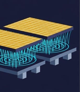
🌋 The Mille-Feuille Curse: HBM's High-Temperature Life-and-Death Struggle
As we all know, when electrical resistance encounters a strong current, heat is generated. What does 1600 watts represent? It's equivalent to concentrating all the heat from a fully operating industrial-grade hairdryer or microwave oven into a tiny chip just a few centimeters square!
If this heat isn't instantly removed, this microscopic city will melt into a puddle of silicon mud within a second.
And in this city, the most fragile and prone-to-collapse defense against high temperatures is not the powerful GPU, but the 8 to 12 seemingly quiet HBM (High Bandwidth Memory) modules next to it.
Why is HBM so sensitive to heat? Please recall how HBM is made: to pack the maximum memory capacity into the smallest possible volume, engineers stack 8, or even 12, DRAM wafers "thinner than hair" like a "French mille-feuille." Then, thousands of tiny TSV (Through-Silicon Via) holes are drilled through these mille-feuille layers, and tens of thousands of micro-bumps are used to firmly solder each layer together.
This is an extremely fragile "Jenga tower."
- Memory Amnesia: DRAM operates by storing electrons in tiny capacitors. When the temperature soars, electrons become active and cause "leakage." If the temperature exceeds a critical threshold, the AI parameters stored within the HBM will instantly vanish, causing the entire AI server to crash.
- Physical Collapse of the Mille-Feuille: This is an even more fatal disaster. When high temperatures arise, each extremely thin silicon wafer begins to "thermally expand and contract." It's like putting a piece of squid on a grill; it instantly curls up (Warpage)! If even one of these 12 layers of chips undergoes a tiny warp, the micro-bump connections in between will immediately be torn apart. A super chip worth tens of thousands of dollars instantly becomes expensive scrap.
🚪 A Fatal Transition: Welcome to the Shura Realm
The CoWoS architecture universe of 5-2-1 concludes at this moment.
We successfully connected chips using CoWoS, but we also opened Pandora's Box, unleashing the demons named "high temperature and warpage."
To save this melting AI brain, traditional packaging technologies are completely obsolete. Global memory giants and OSAT manufacturers must engage in an extremely brutal battle of materials and processes within nano-scale space. Whoever can solve this "high-temperature Jenga" problem will become NVIDIA's most indispensable king.
In-depth Research · Quantitative Perspective
Want to gain more insights from quantitative semiconductor research?
【Insight Subscription Plan】Break Free from Retail Investor Mindset: Build Your Alpha Trading System with "Quantitative Chips" and "Consensus Data"EDGE Semiconductor Research
📍 Series Map — Navigate the Complete EDGE Semiconductor Research →


