Core Takeaway
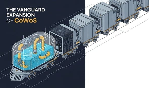
Wet processes are the "first carriage" of capacity expansion: cleaning, photoresist stripping, electroplating, and chemical solution pipelines must be in place first before subsequent photolithography, etching, and packaging can proceed. Amidst the physical bottlenecks of CoWoS-L and thin wafer TB/DB, Grand Plastic (3131) and Scientech (3583) each hold critical choke points.
🏎️ Racing and Car Wash: What is "Wet Process"?
Before delving into the technical intricacies of equipment principles, please imagine an extremely intense F1 racing competition.
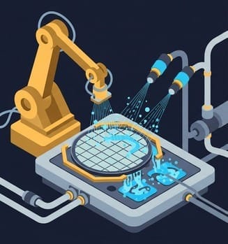
In a semiconductor cleanroom, a wafer costing tens of thousands of US dollars undergoes processes such as "photolithography" (using an exposure machine to print circuits) or "dry etching" (using plasma to remove excess material). Each step is akin to a race car completing a full lap at top speed on a track. After completing a lap, the car's tires will be worn, and its body will be covered in mud and debris. If the car doesn't enter the pit stop at this point to be thoroughly cleaned and equipped with new parts, it will undoubtedly suffer a blowout or crash on the next lap.
Wafers are no different. After TSMC finishes forming TSVs (Through-Silicon Vias) on pure silicon interposers or printing LSI silicon bridge circuits, the wafer surface is left with significant amounts of burnt "photoresist," chemical dust, and metal particles. At this point, the wafer must be sent into a large, enclosed machine, immersed in various extremely dangerous and highly corrosive chemical solutions for "photoresist stripping" and "nanometer-scale cleaning."
Furthermore, as we mentioned in previous chapters, chips need to be connected by tens of thousands of "micro-bumps" and "copper pillars." How do these tiny metal pillars grow? Wafers are immersed in special chemical baths, and an electric current is applied, allowing copper atoms to "electroplate" onto the wafer one by one.
All these steps that require the use of water, chemical solutions, acids, and alkaline solvents are collectively referred to as "wet processes" in the semiconductor industry.
🚂 The "First Carriage" of the Expansion Train
Why is it essential to understand "wet processes" when analyzing the investment logic of semiconductor equipment stocks?
Because wet process equipment represents the "first carriage" in all capacity expansion plans.
Imagine if TSMC were to build a new CoWoS factory today, what would be the first batch of machines they purchase? It would certainly not be the most expensive exposure machines or packaging/assembly machines. Instead, they would first need to lay the "chemical solution pipelines" (chemical supply systems) beneath the factory and prioritize the installation of these large "wet process cleaning machines and electroplating baths."
Without these "car wash" pit stops, subsequent photolithography, etching, and packaging processes cannot even begin to operate. This is why, whenever TSMC or ASE announce an increase in capital expenditure and prepare for major capacity expansion, the revenue and orders (backlog) of wet process equipment manufacturers are always the first leading indicators to show explosive growth.
And on this most critical wet process track, a Taiwanese company has quietly secured a central position in global AI production capacity.
👑 Grand Plastic (3131): TSMC's "Core of the Core"
In the semiconductor equipment supply chain in Taiwan, **Grand Plastic Technology (3131)** is a highly unique entity, even possessing a certain "proud" demeanor.
Through our think tank's in-depth internalization of foreign institutional reports and financial model analysis, we've found that Grand Plastic enjoys exceptionally high price-to-earnings (PE) ratios and stock valuations in the capital market because it possesses two extremely deep moats:
First Moat: Purely In-House High-End Capability, Rejection of 'Low-Margin Agency'
Many equipment manufacturers in Taiwan initially started by "acting as agents" for machines from major foreign manufacturers. While agency business can quickly boost revenue, the gross margin (Gross Margin) is extremely low, essentially earning hard-fought handling and maintenance fees. Grand Plastic, however, is different. It has consistently pursued the arduous path of "100% independent R&D for high-end machines" from start to finish. While this purely in-house business model consumes significant capital during initial R&D, once the machines are certified by customers and begin mass production, their gross margins are exceptionally impressive and lucrative.
Second Moat: A 'Revolutionary Bond' Forged Through Co-Development with Michelin-Starred Chefs
During its advanced packaging R&D, TSMC frequently encountered situations where "no existing machines were available on the market." When TSMC decided to break the limits of photomasks, shatter pure silicon interposers, and invent the extreme "real estate magic" of CoWoS-L (Silicon Bridge Splicing Resin), they faced a massive chemical challenge: What kind of chemicals and washing angles could be used to thoroughly clean those extremely tiny silicon bridges without damaging the delicate resin?
Major foreign manufacturers (such as Japan's DNS or TEL) typically maintain a high stance, unwilling to redesign a customized cleaning machine for a new technology that has not yet entered mass production and carries extremely high risks.
At this critical juncture, Grand Plastic's engineers directly embedded themselves in TSMC's R&D center, working alongside TSMC's PhDs to repeatedly adjust chemical solution formulas and modify machine nozzle designs, eventually developing the exclusive wet process equipment for CoWoS-L.
This is what the industry calls "co-development." Once you have accompanied TSMC through this challenging journey of R&D from scratch, your machine parameters become firmly "locked into" TSMC's Process of Record (POR).
Therefore, as TSMC prepares to fully commit its massive CoWoS capacity of up to 150,000 wafers per month to CoWoS-L technology in 2026; as the exclusive/primary supplier of CoWoS-L wet process equipment, Grand Plastic has naturally become the "core of TSMC's core" in this wave of AI capacity expansion.
🧻 The Dilemma of the Wet Wipe: Why Grind Wafers Thinner Than Paper?
Before delving into this astonishing procedure, we must first understand a major premise: why do engineers subject perfectly good silicon wafers to such a fragile state?
In Chapter 5-2-2, we discussed the "HBM layering battlefield." To stack 12 chips together while ensuring efficient dissipation of the thousands of watts of heat generated by the GPU, the chips themselves cannot be too thick (thickness impedes heat dissipation and increases volume).
Therefore, before advanced packaging, wafers must undergo a process called "Backside Grinding."
Engineers use extremely hard diamond grinding wheels to relentlessly grind down a 12-inch silicon wafer, originally over 700 micrometers ($\mu m$) thick, until its thickness is less than 50 micrometers!
What does 50 micrometers mean? A standard A4 printer paper used in your office is approximately 100 micrometers thick. This means that this AI wafer, costing tens of thousands of US dollars, is ground down to an extreme state, "half as thin as paper."
Silicon is inherently a very brittle material (like glass). When ground to just 50 micrometers, it becomes like a "water-soaked wet wipe." If the robotic arm in the cleanroom grips it slightly too hard, or if there's too much air resistance during movement, this 12-inch wafer could instantly shatter into thousands of pieces of scrap, like a potato chip, in mid-air!
Given that this wafer shatters at the slightest touch, how do engineers manage to send this "wet wipe" into machines filled with strong acids, alkalis, and high temperatures for complex processing like TSV drilling and copper pillar growth?
🩹 The Magic that Saves Fragile Wafers: TB/DB (Temporary Bonding / De-Bonding)
To solve this physical impasse, the semiconductor industry invented a rescue technology that can only be described as "magic," fully named TB/DB (Temporary Bonding / De-Bonding).
The logic of this technology is remarkably simple yet its execution is hellishly difficult:
Step One: TB (Temporary Bonding, sticking the wet wipe to a board)
Since the thin wafer is too fragile to handle, engineers use a "Glass Carrier" that is 700 micrometers thick.
Then, a highly specialized "Polymer Adhesive" (double-sided tape) is applied between the thin wafer and the thick glass, bonding them firmly together.
With this thick glass serving as a "skeleton and support," the thin wafer, which was previously prone to shattering, instantly becomes incredibly rigid. Now, it can be confidently sent into any high-temperature, high-pressure wet process or etching machine for intense processing.
Step Two: DB (De-Bonding, peeling off the double-sided tape)
Once all CoWoS processing is complete and the micro-bumps are fully formed, the most terrifying moment arrives.
Engineers must "separate" (peel off) this ultra-thin, processed wafer from the thick glass carrier.
This is the most nerve-wracking second in the entire packaging process.
🧨 The Extreme of Tape Peeling: The "One Second" Worth Hundreds of Millions of New Taiwan Dollars
Imagine this: the "double-sided tape" has just endured high-temperature baking at two or three hundred degrees Celsius, and has been immersed in various strong acids and alkalis; it's already bonded firmly.
Now, a machine needs to "peel" a silicon wafer, thinner than paper and etched with NVIDIA's top-tier AI chips, from this thick glass.
- If the peeling force is slightly too strong? Snap! The wafer instantly splits in half.
- If the peeling angle is off by even one micrometer? Stress will build up at the wafer edge, causing it to shatter instantly.
- If even a tiny bit of double-sided tape residue remains on the wafer surface? All subsequent packaging connections will fail, rendering the entire chip worthless.
To solve this problem, current DB (De-Bonding) machines first emit a highly precise "laser beam" that penetrates the transparent glass and accurately hits the adhesive layer, causing the glue to instantly lose its stickiness (carbonization). Then, the machine uses extremely gentle suction cups and a peeling mechanism, applying almost "baby-like" uniform force, to carefully lift this priceless thin film wafer.
This machine, responsible for "bonding and de-bonding the tape," is the most fragile physical defense at the choke point of capacity expansion.
🛡️ Scientech (3583)'s Breakthrough: The Game-Changer that Controls the Physical Choke Point
On this extremely perilous "tape peeling" battlefield, foreign equipment giants (such as Austria's EVG or Germany's SUSS) have long held a monopoly. No foundry dared to entrust wafers worth hundreds of millions to an unproven local equipment manufacturer for "peeling."
However, as TSMC's CoWoS capacity faced an explosive demand of 150,000 wafers, the lead times and exorbitant prices of foreign equipment could no longer meet TSMC's expansion speed.
This presented another major wet process equipment company in Taiwan – **Scientech (3583)** – with a once-in-a-lifetime historical opportunity.
Through long-term R&D and rigorous testing on TSMC's production lines, Scientech successfully broke through the patent barriers of foreign competitors, developing its own TB/DB (Temporary Bonding/De-Bonding) in-house equipment!
Scientech's machines not only perfectly execute the precise peeling action of laser de-bonding but also demonstrate extremely high yield rates in wafer cleaning and chemical removal, successfully integrating into the core supply chain for TSMC's CoWoS expansion.
Scientech has effectively seized control of the physical choke point in the CoWoS process where shattering disasters are most likely to occur. As long as TSMC's advanced packaging requires wafer thinning, Scientech's TB/DB machines serve as the irreplaceable ultimate safeguard.
⚖️ Two Different Money-Printing Machines: Boutique Store vs. High-End Department Store
In the fiercely competitive semiconductor equipment market, key metrics for evaluating a company's value, beyond "revenue scale," are "gross margin" and "revenue diversification." Grand Plastic and Scientech represent the two extremes of this spectrum.
Grand Plastic (3131)'s "Boutique Store Philosophy": Purely In-House & High-End Exclusivity
Grand Plastic's business model is akin to a "haute couture boutique" serving only top-tier VIPs. They are extremely resistant to low-margin "agency" business (selling machines for foreign manufacturers), insisting on investing all R&D resources into "100% independent R&D" for wet process and electroplating machines.
This approach is very challenging during normal times due to extremely high R&D expenses. However, when TSMC sought to develop the most cutting-edge and difficult CoWoS-L (Silicon Bridge Splicing Resin), and no existing machines were available on the market, only Grand Plastic was willing and able to "co-develop" with TSMC in the laboratory. Once the equipment is successfully developed and locked into TSMC's Process of Record (POR), Grand Plastic effectively secures "exclusive supply rights" for this high-end equipment. Since no competitors can immediately replicate such customized machines, Grand Plastic enjoys exceptionally strong pricing power, leading to its outstandingly high gross margins among equipment stocks. Grand Plastic profits from the "monopoly on cutting-edge technology."
Scientech (3583)'s "Department Store Strategy": Core Flagship Product + Comprehensive Peripheral Coverage
In contrast to Grand Plastic's singular focus, Scientech demonstrates an extremely flexible and aggressive business approach. Scientech's revenue structure is a perfect "combination punch":
- Core Flagship Product (In-house TB/DB): As mentioned in the previous section, Scientech successfully broke through foreign competition to produce the most challenging "tape peeling (temporary bonding/de-bonding)" machines. This in-house developed equipment is the core engine of Scientech's gross margin and technological leverage.
- Agency Support (High-end Equipment Agency): Scientech has not abandoned its agency business. They represent top global semiconductor measurement and analysis equipment. While agency business has lower margins, it generates stable and substantial cash flow and allows Scientech's sales force to stay updated on the latest expansion trends at foundries.
- Beneficiary of Capacity Spillover: When TSMC allocates high-end wet process orders to Grand Plastic to meet the massive demand for 150,000 CoWoS wafers, a significant "spillover effect" occurs for the relatively mature wet process equipment demands within TSMC's fabs (e.g., CoWoS-S or traditional packaging). Scientech, with its excellent cost-performance ratio and flexible capacity, naturally secured these large spillover orders.
Scientech profits not only from its core technology but also from the "comprehensive benefits of scale expansion and capacity displacement."
🌊 A "Win-Win Scenario" Under the 150,000 Wafer Capacity Tsunami
Understanding these two distinct business logics helps us comprehend why both companies are highly favored by recent foreign institutional reports and within the institutional investment community.
Facing the advanced packaging capacity tsunami of up to 150,000 wafers per month (150k wfpm) by 2026, TSMC's appetite is too immense for any single equipment manufacturer to satisfy alone.
- TSMC needs Grand Plastic to ensure that the most cutting-edge and precise CoWoS-L chips of the future can be perfectly cleaned and electroplated;
- TSMC also relies heavily on Scientech to ensure that those tens of thousands of ultra-thin wafers do not shatter during de-bonding, and to supplement the quantitative gap in the entire wet process defense line with Scientech's substantial capacity support.
In this capacity expansion project, Grand Plastic sells the most expensive "precision cranes," while Scientech provides the indispensable "specialized excavators" and a vast fleet of engineering vehicles. These two Taiwanese domestic equipment suppliers have not only successfully conquered the equipment strongholds previously dominated by Japan (DNS, TEL) and Europe (SUSS, EVG) but have also, driven by the surge in AI, entered their most glorious golden era in thirty years of operation.
In-Depth Research · Quantitative Perspective
Want more semiconductor quantitative research insights?
【Insight Subscription Plan】Break Free from Retail Investor Mentality: Build Your Alpha Trading System with 'Quantitative Chips' and 'Consensus Data'EDGE Semiconductor Research
📍 Series Map — Navigate the Complete EDGE Semiconductor Research →


