5-2-4 Die Bonder: The Ultimate Micron Showdown – Global Hegemons vs. Taiwan's Wonbond (6187) and Jinhua (6640) Carving Out Their Niche
Die bonder challenges in packaging: Surging AI chip value mandates micron-precision thermocompression bonding, high barriers. Dutch Besi (hybrid bonding) & HK's ASMPT (advanced packaging) dominate. Taiwan's Wonbond and Jinhua seek niche breakthroughs, vying with foreign hegemons for packaging.
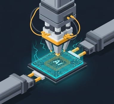
🥼 The Most Expensive Operating Table: What is a Die Bonder (Die Attach)?
In the semiconductor packaging process, the action of picking up diced small chips (Die) and attaching them to a substrate or interposer is called Die Attach. The large machine responsible for performing this action is called a Die Bonder.
If you thought this was as simple as a robotic arm in a factory or a claw machine at a night market, merely picking up and placing a chip, you would be gravely mistaken.
In traditional low-end chip packaging, the Die Bonder's actions are indeed relatively simple. However, we are now dealing with NVIDIA's top-tier AI chips, each costing tens of thousands of US dollars! This is a "microscopic neurosurgery" that allows for no mistakes and must succeed on the first attempt.
🔬 Life and Death in One Micron: Extreme Alignment to One-Tenth the Diameter of a Red Blood Cell
Let's examine just how terrifyingly difficult this operation is.
First, beneath the "belly" of this massive GPU chip, tens of thousands of densely packed "micro-bumps" are arrayed. On the foundation (silicon interposer), there are also tens of thousands of corresponding tiny metal contacts.
The Die Bonder's first task is to suspend this chip in the air and then align it using an extremely precise optical lens.
What is the alignment tolerance? The answer is: it cannot exceed 1 micron ($mu m$)!
What does 1 micron mean? A human hair is approximately 50 to 100 microns in diameter; a red blood cell in the human body is about 8 microns in diameter.
In other words, this massive mechanical equipment must, while suspended in mid-air, align tens of thousands of micro-bumps on the chip with the contacts on the foundation with "100% perfect fit," using a precision scale of "one-tenth the diameter of a red blood cell." Even the slightest tremor, a misalignment of just half a micron, would cause these tens of thousands of contacts to "misalign and short-circuit," rendering this multi-thousand-dollar super-brain instantly brain-dead.
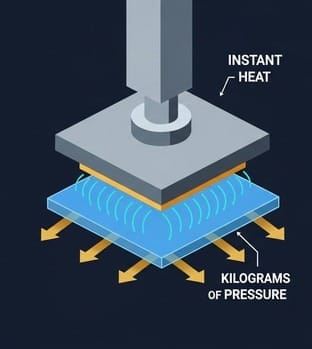
⚖️ The Paradox of Destruction and Rebirth: The Physical Magic of Precise Pressure Application
But merely aligning is not enough; the most counter-intuitive physical challenge lies in the moment of "placement."
To ensure these tens of thousands of micro-bumps perfectly interlock and conduct electricity with the underlying contacts, the Die Bonder must, at the moment of bonding, apply immense pressure of up to several kilograms (Kilograms) onto the chip from above, while simultaneously heating it instantly to melt and connect the metal contacts (this is known as TCB (Thermo-Compression Bonding)).
At this point, a fatal physical paradox emerges:
Do you recall that we mentioned in a previous chapter how these AI chips are ground extremely thin and fragile for heat dissipation?
Now, the Die Bonder is tasked with pressing several kilograms of force onto this silicon chip, which is as thin as a cicada's wing and shatters at the slightest touch!
If the robotic arm's downward pressure differs by just a fraction of a gram between the left and right sides of the chip, or if the pressing speed isn't perfectly buffered in the last millisecond... "CRACK!" – this fragile super-chip would instantly shatter under the immense pressure, turning to dust.
This machine must possess both the "overwhelming force of Mount Tai" and the "gentleness of a falling feather," ensuring that while applying immense pressure, the force is distributed 100% uniformly across every nanometer corner of the chip.
👑 The Crown Jewel of Semiconductor Mechanical Engineering
Precisely because it must simultaneously handle "extreme precision," "terrifying high temperatures," and "absolutely uniform heavy pressure" within the confined space of 1 micron, the Die Bonder has become the "crown jewel" of the entire semiconductor back-end packaging process, commanding the highest unit price, possessing the deepest technological barriers, and featuring the most complex mechanical design.
It is an ultimate weapon that pushes human mechanical engineering, optical alignment, and fluid dynamics to their absolute limits.
🧱 The Cruel Reality: Why TSMC Dares Not Replace Them?
To understand the industry landscape of Die Bonders, we must first move beyond the myth of "technical parameters" and return to the most authentic "business calculations."
In the procurement logic for semiconductor equipment, there is an unwritten iron rule: "Cost reduction and efficiency improvement must never be built upon the risk of destroying super-chips."
Please imagine an extreme scenario: Suppose today a local equipment manufacturer in Taiwan, having dedicated all its efforts to developing a Die Bonder with specifications comparable to foreign competitors and a 30% lower price, eagerly approaches TSMC for a sales pitch. Would TSMC's plant manager make the purchase?
Absolutely not.
Because the moment this Die Bonder prepares to press down, it is handling an NVIDIA B200 chip module costing between 30,000 and 40,000 US dollars. If this new local machine, due to prolonged operation, develops minor metal fatigue, causing the downward pressure to increase by just one gram, and instantly crushes this super-brain, would the saved equipment price difference of several million NTD be enough to compensate for this single chip? If ten chips are crushed in a day, the entire production line's monthly profit would evaporate!
This is the semiconductor industry's most brutal "Wall of Trust." Foundries are like hospital directors at top-tier hospitals; when they perform brain surgery for the world's wealthiest VIP clients, they only dare to hire "master surgeons" with thirty years of flawless records, never cheap interns.
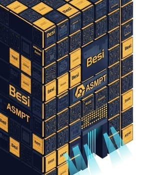
Looking across the global advanced packaging industry, only two companies can be called master surgeons: the Netherlands' Besi (Besi Semiconductor) and Hong Kong's ASMPT (Advanced Semiconductor Materials Pacific Technology).
👑 The Supreme King Besi (Netherlands): Absolute Dominance in Hybrid Bonding
If you follow the trends of European tech stocks, you'll undoubtedly be impressed by Besi's (Amsterdam Exchange Ticker: BESI.AS) rocket-like stock price surge over the past few years.
According to highly confidential data recently internalized by our think tank from top European investment banks, Besi currently holds a despairingly absolute dominance in the most advanced Die Bonder segment, especially in next-generation "Hybrid Bonding" technology, which is regarded as the physical holy grail.
150 Machines: A Moat of Real-World Experience: While other competitors are still experimenting in laboratories, Besi's Hybrid Bonding machines have already shipped over 150 units to major top-tier foundries worldwide! The yield data and fine-tuning parameters collected daily from these 150 machines on production lines are priceless treasures that no latecomer can acquire, no matter how much money they spend.
Terrifying Precision of 50 Nanometers: In our previous article, we stated that 1 micron (1000 nanometers) is the line between life and death. However, according to the latest intelligence, Besi is prepared to advance the precision of its newest generation of equipment directly to the terrifying realm of 50 nanometers (50nm)!
Super Orders for HBM4: As memory enters the next generation of HBM4 and HBM4E, existing stacking technologies are nearing their limits. Besi, leveraging its overwhelming technological advantage, is poised to fully capture the large orders for TCB and Hybrid Bonding equipment that memory giants are compelled to upgrade to combat high temperatures.
Besi, like a supreme monarch wielding the most precise laser scalpel, firmly occupies the highly profitable top tier of the semiconductor pyramid.
🐉 Overlord's Counterattack: ASMPT (0522.HK): "Subtraction Strategy" and All-Out War
Facing Besi's strong dominance, the former global packaging equipment overlord – ASMPT (Hong Kong Stock Exchange Ticker: 0522.HK) – will certainly not sit idly by.
Through our in-depth analysis of ASMPT's recent internal strategies and foreign investment revaluation reports, we have discovered that this slumbering Eastern giant is launching an industry-shaking "Subtraction Strategy (Addition to Subtraction)."
In the past, ASMPT's business was highly complex; besides semiconductor packaging, they also had a substantial traditional SMT (Surface Mount Technology, used for mounting components onto printed circuit boards) business. However, catalyzed by the AI frenzy, ASMPT's board of directors made an extremely decisive choice:
They are actively evaluating the "divestiture or spin-off" of their traditional SMT business!
This is a highly explosive strategic signal. This means ASMPT is preparing to concentrate 100% of the group's R&D resources and cash flow entirely on the ultimate track of "Semiconductor Advanced Packaging (SEMI)."
Freed from the burden of traditional businesses, ASMPT has demonstrated extremely fierce aggressiveness:
Absolute Counterattack in TCB (Thermo-Compression Bonding): In the TCB market for logic chips, ASMPT is rapidly reclaiming lost ground. Leveraging its strong production capacity and tuning capabilities, it has become the most potent weapon to counterbalance Besi's dominance on advanced packaging lines at TSMC and other foundries.
Striking Directly at the Heart of SK Hynix: According to the latest intelligence we've obtained, ASMPT has successfully broken through in the intensely competitive HBM4 equipment battle, securing critical TCB machine orders from SK Hynix! This is akin to forcibly tearing open a bloody gap in the territory of Besi and local Korean equipment manufacturers (such as Hanmi Semiconductor).
This Die Bonder holy war, led by Dutch and Hong Kong giants, has not only boosted their own valuations but has also pushed the technological barriers of advanced packaging to the absolute limits of human mechanical engineering.
🧮 The Deadly Math Problem: What is "KGD (Known Good Die)"?
Before NVIDIA's GPUs and SK Hynix's HBM are sent into Besi's bonding machines, we must first confront a term that sends shivers down the spine of the advanced packaging industry: KGD (Known Good Die).
Why is KGD so important? Let's calculate an extremely brutal yield math problem.
In traditional packaging, a chip is encased in a plastic shell; if the chip is inherently bad, the loss is merely that chip and a small, inexpensive packaging fee.
But CoWoS is completely different! Now, we are placing 1 super GPU and 8 HBM chips simultaneously onto an extremely expensive pure silicon interposer.
Assume that before these 9 chips are sent into the bonding machine, their individual yields are as high as 98% (which is an excellent figure in the semiconductor industry).
Then, what would be the overall yield of this CoWoS module once these 9 chips are assembled together?
The answer is: $0.98^9 = 0.83$ (83%).
Do you understand this terrifying "yield multiplier effect"? If any single small chip placed in is bad, even if the other 8 chips are perfectly flawless top-tier chips, this entire AI brain, costing tens of thousands of US dollars, will instantly turn into useless, expensive scrap metal!
While Besi and ASMPT's Die Bonders are incredibly precise, they are essentially "blind surgeons." The bonder only "picks up and presses down"; it has no idea whether the chip it's handling is a genius or an imbecile.
Therefore, before the operation begins, someone must meticulously inspect tens of thousands of newly diced chips, one by one, using an extremely precise magnifying glass. All defective chips must be discarded, and only those "confirmed to be flawless KGD (good dies)" are neatly arranged and sent to the operating table.
This extremely sacred and unforgiving task, where not a single error is permitted, is called "Die Sorting."
🥢 The Claw Machine at the Physical Limit: The Hellish Difficulty of the Chip Sorter
The equipment responsible for performing this task is called a Chip Sorter.
If you think "sorting" sounds like a low-level classification job, then you have severely underestimated the limits of physics.
Recall from chapter 5-2-3 that after back-grinding, these wafers are less than 50 microns thick, thinner and more brittle than a wet tissue.
These wafer-thin chips, after being separated by laser dicing, stick to a sticky "blue film (dicing tape)."
Jinhua's sorter must perform the following breathtaking sequence of actions on this blue film:
Reading the Death List: The machine must first connect to the foundry's database to read the "digital map (Wafer Map)" of this wafer, identifying which dies are failed units and which are true KGDs.
The Life-or-Death Game of Ejector Pin and Vacuum Nozzle: When the machine identifies a KGD, an extremely fine metal "ejector pin" underneath gently "pushes" this ultra-thin chip upwards from below the blue film; simultaneously, an extremely precise "vacuum nozzle" above "sucks" the chip upwards.
Non-Shattering Separation: This is a tug-of-war against the stickiness of the blue film. If the ejector pin below pushes too hard, invisible "micro-cracks" can form within the chip; if the vacuum nozzle above sucks too forcefully, the chip can experience "warpage."
Ultimate Six-Sided Visual Judgment: After successful pickup, the chip flies through a set of ultra-high-speed AOI (Automated Optical Inspection) lenses in mid-air at millisecond speeds. Within this thousandth of a second, the lenses must inspect all six sides of the chip for any scratches or chipped corners.
Precise Storage: Finally, this confirmed perfect chip is gently placed into a specialized carrier (Tape & Reel or Waffle Pack), ensuring its rotational angle and center position are absolutely precise (typically within a few microns of tolerance), so that the subsequent Besi bonder can pick it up blindly.
Jinhua's machines must repeat this action thousands to tens of thousands of times per hour, and "are not allowed to break any chip."
🛡️ Jinhua's (6640) Ultimate Moat: From "Cost-Effectiveness" to "Production Line Guardian"
In the past, the chip sorter market also had many Japanese or European competitors. But why has Jinhua (6640) been able to emerge from this tsunami of AI production expansion with an overwhelming market share (estimated by the industry to be over 70% in advanced packaging in Taiwan), becoming TSMC's most trusted ultimate guardian?
This is not merely due to "low prices (high cost-effectiveness)," but because Jinhua has built an unparalleled "supply chain ecosystem moat."
This post is for subscribers only
Sign up now to read the post and get access to the full library of posts for subscribers only.