🌋 Fatal Physical Deformation: When Three Extreme Materials Are Forced Together
To understand this catastrophe, we must first grasp what has been crammed onto this 12-inch CoWoS wafer.
On this paper-thin substrate, engineers, in pursuit of ultimate performance, have forcibly bonded three materials with completely different physical properties:
- Silicon: This includes the underlying silicon interposer and the GPU and HBM chips themselves.
- Copper: This comprises tens of thousands of micro-bumps and the copper pillars within TSV (Through-Silicon Via).
- Organic Polymer: This includes the underfill recently dispensed by Wanrun, and the molding compound used to encapsulate the entire chip.
At this point, the most unforgiving and difficult-to-overcome constant in physics makes its appearance: the Coefficient of Thermal Expansion (CTE).
What is CTE? Simply put, it's "the degree to which an object expands significantly when heated and contracts when cooled."
Among these three materials, silicon is the most stable; its volume hardly expands or contracts regardless of temperature changes. Copper is moderately responsive, exhibiting noticeable expansion and contraction with temperature. However, the organic resin (plastic glue) after liquid hardening is extremely volatile! As soon as the temperature rises, it expands rapidly; as soon as the temperature drops, it contracts drastically.
These three materials are now tightly bonded together with glue, with no room for compromise!
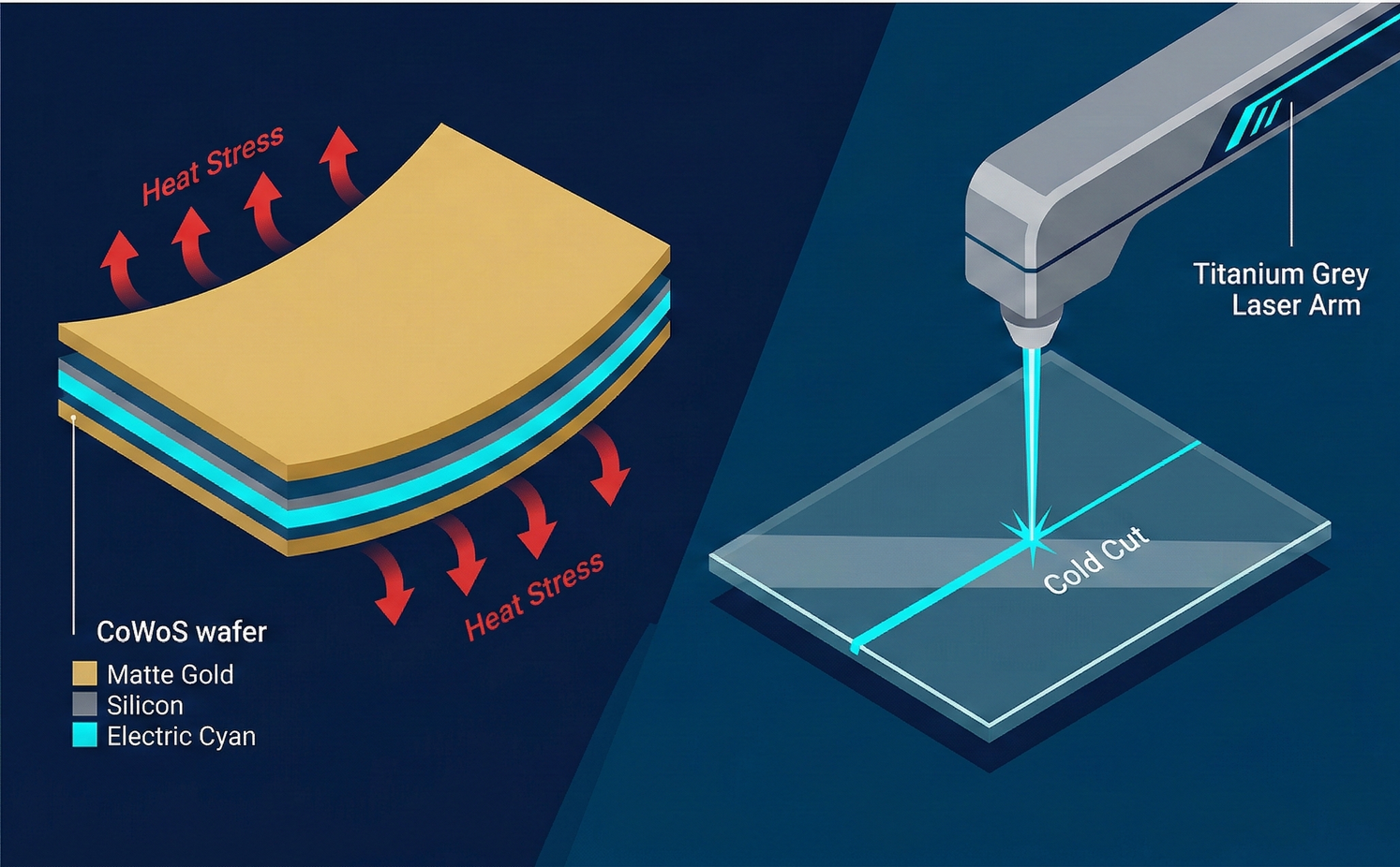
🦑 A Multi-Million Dollar "Grilled Squid": The Phenomenon of Warpage
When the temperature inside the machine is above 200 degrees Celsius, the plastic glue is in a melted and expanded state, and all is well.
However, once processing is complete and this 12-inch wafer is removed from the machine, disaster strikes as it slowly cools down to room temperature (25°C).
The organic resin begins to "contract wildly and drastically," but the silicon chip beneath it "remains unmoving, refusing to contract."
The resin pulls inward desperately, while the silicon chip holds firm. These extremely uneven tensile forces from contraction (known in the industry as internal residual stress) are all concentrated on this fragile wafer, which is less than 50 micrometers thick.
What does this look like?
It's like throwing a thin-crust pizza loaded with rich toppings, or a fresh squid, directly onto a hot grill!
Under the uneven forces of heating and cooling, the entire 12-inch wafer, which should have been perfectly flat, uncontrollably warps upward (like a smiling bowl) or bends downward (like an inverted dome)!
In the advanced semiconductor packaging industry, this is known as the most dreaded archenemy—Warpage.
💥 Chain Reaction of Cracking and Jamming
You might think: "What's the big deal if the wafer is slightly bent? Can't you just flatten it?"
In a nano-scale cleanroom, this is absolutely fatal.
- Robotic Arm Failure: All automated transfer equipment (OHT, robotic arms) in a wafer fab are designed with the assumption that wafers are "perfectly flat." If the edge of this 12-inch wafer warps by more than a few millimeters (mm), the robotic arm cannot precisely grip it. The wafer will directly jam in mid-air during transfer, or even fall and shatter.
- Vacuum Chuck Failure: The machine for the next process step must firmly hold the wafer with a vacuum chuck for processing. If the wafer is bent (like a leaky bowl), the vacuum simply cannot hold it. If brute force is used to flatten and hold it...
- Internal Fracture: With a "snap!", the enormous stress accumulated inside the wafer, with nowhere to dissipate, will instantly tear off tens of thousands of metal micro-bumps inside the chip, or even cause the silicon chip to stress fracture like glass!
As soon as severe warpage occurs, this 12-inch wafer, carrying dozens of NVIDIA's top-tier AI chips and worth over NT$100-200 million, will instantly become worthless industrial scrap.
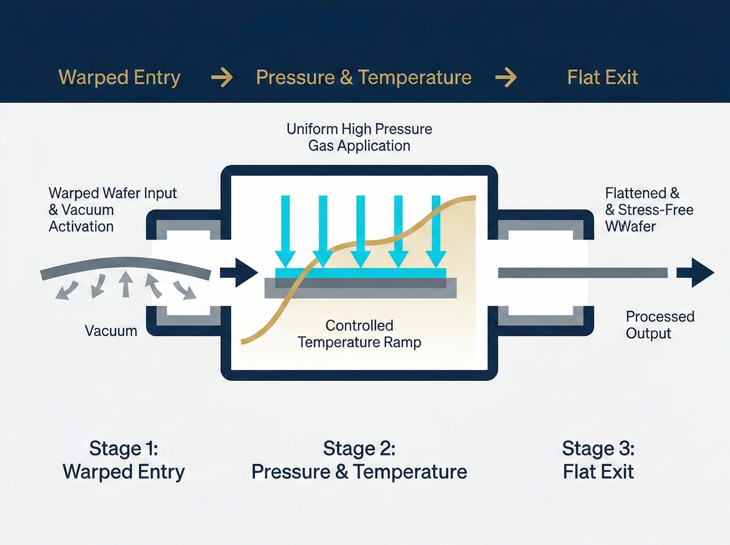
🧖♂️ The Chip's Extreme Sauna: The "Ironing" Magic of VPO (Vacuum Pressure Oven)
What's the best way to calm a curling grilled squid? The answer is: give it an extremely precise "sauna SPA."
In the back-end process (oS side) of CoWoS, after Wanrun dispenses the underfill or applies the molding compound, this wafer is immediately sent into C-Sun's ace equipment—the VPO (Vacuum Pressure Oven).
The operational logic of this oven is a perfect combination of thermodynamics and materials science:
- Extreme Vacuum (Void-free): After the wafer is loaded, the machine first evacuates all air, reaching an extremely high vacuum state. This step aims to force out all "micron-sized voids" hidden in the glue gaps, completely eliminating the bubble bombs we mentioned in the previous chapter.
- Precise Pressurization and Heating: Next, the machine injects high-pressure nitrogen gas, applying an "absolutely uniform gas pressure" to the wafer surface, while simultaneously beginning to slowly and precisely increase the temperature.
- Golden Curve for Stress Release: This is C-Sun's core secret (Know-how). C-Sun's oven doesn't just simply raise the temperature; it strictly follows a "Baking Profile" discovered through countless experiments. It gives the polymer resin sufficient time to "release internal stress" during the melting, cross-linking, and final solidification stages.
Through this perfect synergistic operation of vacuum, pressure, and temperature, C-Sun effectively "digests" the contraction and pulling forces between each material layer.
When the wafer is removed from C-Sun's VPO oven and cooled to room temperature, it's like a silk shirt perfectly "ironed" by a high-temperature steam iron, regaining an incredibly absolute flatness. The warpage crisis is declared over!
🤝 The Ultimate Art of Collaborative Warfare: The Ecosystem Barrier of the "G2C+ Alliance"
You might ask: "While oven technology sounds difficult, aren't there major foreign manufacturers who can do it? Why does TSMC have to use C-Sun?"
This touches upon the most formidable business strategy of equipment manufacturers in Taiwan in the advanced packaging battle—"collaborative warfare (ecosystem binding)."
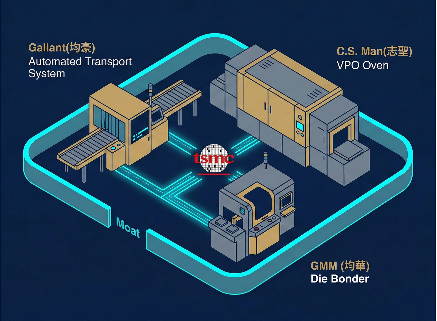
As our think tank deeply deciphers the global semiconductor supply chain, we discovered that C-Sun's strength lies not only in itself but also in the unbreakable "G2C+ Alliance" behind it.
In 2020, C-Sun (2467) brought in semiconductor automation giant GPM (5443) and TOPCO (6640), the "ultimate gatekeeper for KGD" that we introduced in the previous chapter. These three companies formed a formidable alliance, a fleet with cross-firepower.
Please imagine this scenario:
When TSMC's R&D博士 (Ph.D.) is developing the next generation of even larger CoWoS-L, they discover that the existing process leads to severe warpage. At this point, if they were to seek foreign suppliers, TSMC would have to call American automation companies, Japanese bonding machine manufacturers, and European oven manufacturers separately, asking them to fly to Taiwan for meetings, which would be time-consuming and protracted.
But with the G2C+ Alliance, TSMC only needs one meeting!
- GPM is responsible for modifying the front-end automated transfer (to prevent bent wafers from falling).
- TOPCO adjusts the bonding parameters of the Die Bonder.
- C-Sun, in the final stage, immediately customizes a brand-new VPO oven with a new temperature control curve.
Engineers from all three companies directly move into TSMC's fabs, working 24 hours a day, seamlessly resolving this physical deadlock caused by warpage.
This "one-stop collaborative operation and localized R&D" directly locks C-Sun's oven parameters into TSMC's standard process (POR). This moat built by the ecosystem is so deep that even foreign equipment giants cannot cross it.
🚀 Beyond the Silicon Boundary: WMCM, SoIC, and the Ultimate Setup for Panel-Level Packaging
Stepping beyond short-term financial figures, if we view C-Sun from a "God's eye perspective" of industrial evolution, we'll find that C-Sun has formally transcended the boundary of a "traditional PCB equipment manufacturer" and magnificently transformed into a highly pure "advanced packaging arms dealer."
Based on our understanding of the technology roadmap, C-Sun's thermal processing magic has comprehensively positioned itself for the ultimate battlegrounds of the next three to five years:
- Apple's Next-Generation Weapon (WMCM): According to the latest supply chain intelligence, Apple is expected to abandon the traditional InFO process for future iPhone 18 processors, adopting an entirely new WMCM (Wafer-Level Multi-Chip Module) advanced packaging. C-Sun has successfully secured a large order for heating equipment for this new production line.
- The Pinnacle of 3D Stacking (SoIC): In the field of SoIC (System-on-Integrated-Chips), where there are no bumps and copper-to-copper direct bonding is used, C-Sun's equipment has also entered the supply chain.
- Absolute Dominance in Panel-Level Packaging (CoPoS / FOPLP): This is the most terrifying breakthrough point! When advanced packaging shifts from "12-inch circular silicon wafers" to "extra-large rectangular glass panels," traditional semiconductor equipment manufacturers are all stunned because they have never dealt with such large pieces of glass! But C-Sun started as a panel equipment manufacturer! C-Sun possesses the deepest technical expertise globally in handling glass substrate warpage, baking, and temperature uniformity control. Future panel-level packaging (CoPoS) is simply C-Sun's absolute home turf for a dimension-reducing strike!
⚔️ The Light Blade of Zero Physical Pressure: Laser Modification and Cold Cutting
In the semiconductor cleanroom, the ultimate wizard who controls this "light" is Taiwan's major laser and plasma equipment manufacturer—T-Laser (8027).
In T-Laser's revenue structure, over half (52.93%) of its contribution comes from its most proud "laser equipment."
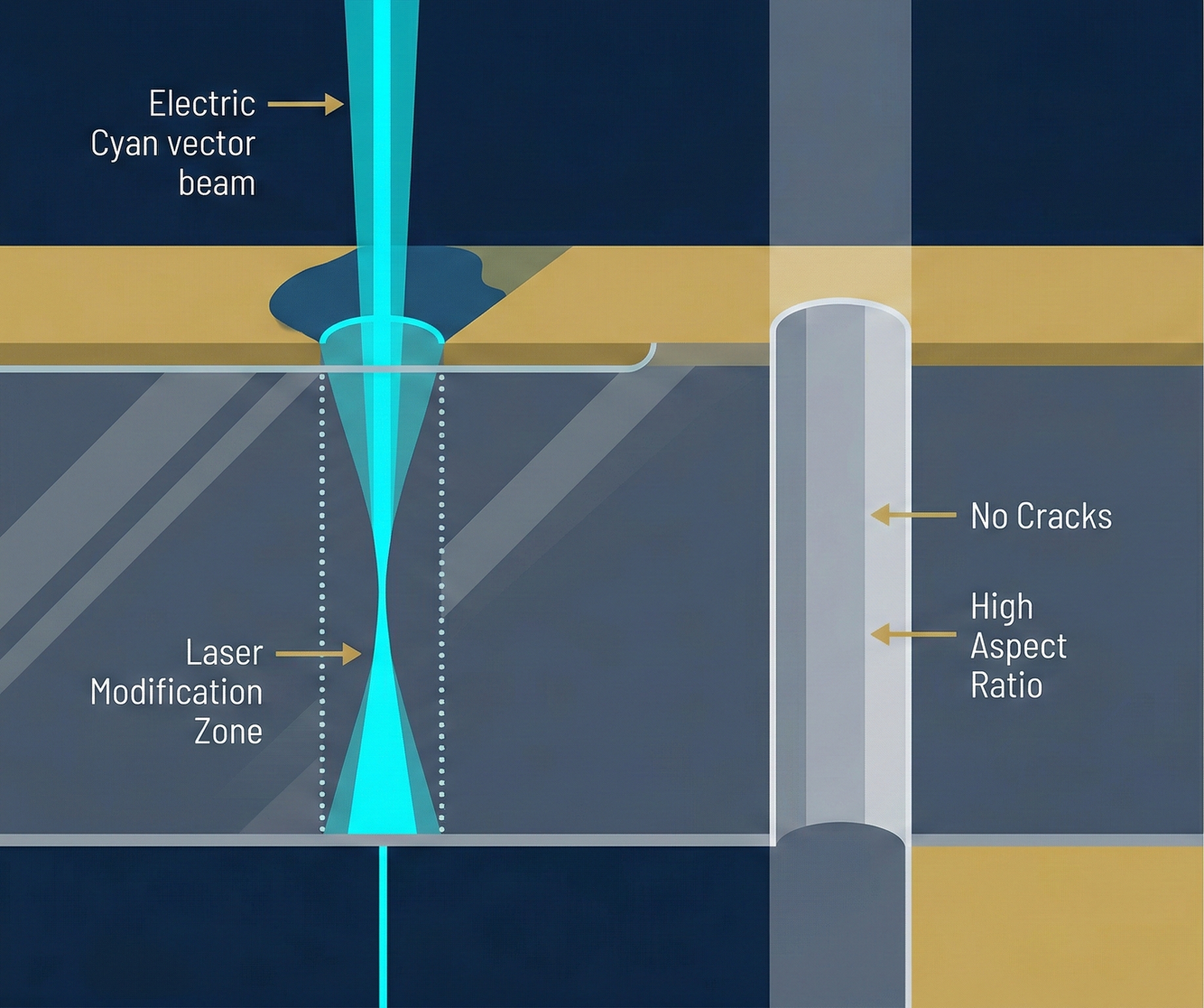
When dealing with extremely fragile composite materials like CoWoS, T-Laser's machines do not emit physical blades, but rather extremely high-frequency "ultrashort pulse lasers (such as picosecond or femtosecond lasers)."
This is a processing technology that borders on science fiction:
- Sublimation and Vaporization: The moment the laser beam focuses on the wafer, the powerful energy directly breaks the chemical bonds of the material. The material doesn't even have time to melt; it directly "vaporizes" from a solid into a gas and is drawn away.
- Zero Heat Affected Zone (HAZ): Because the pulse duration is extremely short (one millionth of one millionth of a second), heat simply does not have time to conduct to adjacent chips, hence it is referred to as "cold cutting."
- Laser Modification: T-Laser's laser can even penetrate the wafer surface, precisely destroying the material structure (modifying it) "inside" the wafer. Then, with a gentle pull, the chip will perfectly break along the invisible dotted line drawn by the laser, with edges as smooth as a mirror, completely avoiding any corner chipping risk associated with physical blades.
This is T-Laser's core value in the CoWoS battle: "Achieving the most critical precise cutting without wafer warpage and without applying any physical pressure."
⬛ The Future Battlefield of Dimension-Reducing Strikes: The Overlord of FOPLP (Fan-Out Panel Level Packaging)
However, if we only see T-Laser as a cutting machine supplier on the CoWoS production line, we would be greatly underestimating the company's strategic vision.
Through our think tank's deep assimilation of top institutional investors' confidential reports, we discovered that T-Laser's true "nuclear-level breakthrough point" is not on traditional 12-inch circular wafers at all, but on the "super-large square glass and metal panels" that are about to revolutionize the entire industry!
This future technology is called FOPLP (Fan-Out Panel Level Packaging).
When TSMC and global packaging manufacturers realized that the area of 12-inch wafers was no longer sufficient to accommodate more GPUs, they decided to replace the packaging substrate with giant square panels measuring up to 700mm * 700mm!
But this created a huge disaster: traditional semiconductor equipment manufacturers' machines were all designed for "circular shapes with a diameter of 300mm," and they simply could not handle this super-large 700mm square!
This presented T-Laser with a once-in-a-lifetime historical opportunity.
According to the latest industry intelligence we have, T-Laser's FOPLP-specific equipment (including plasma cleaning, plasma etching Descum, and laser cutting) has demonstrated extremely powerful dominance.
In the second half of 2025, they had already begun shipping these giant machines to top-tier North American clients, with end applications directly targeting the hottest areas of HPC (High-Performance Computing) and low-earth orbit satellite chips.
Even more astonishing, this wave has just begun, and it is expected that T-Laser's FOPLP equipment will add two more heavyweight clients in 2026!
💎 TGV (Through-Glass Via): The Ultimate Black Technology That Pierces Limits
If FOPLP is the next-generation battlefield, then "Glass Substrate" is the "ultimate holy grail" of semiconductor materials for the next decade.
Future AI chips transmit data so fast that traditional organic plastic substrates cause severe signal loss. Intel and major US manufacturers have decided: future superchips must be built on "pure glass"!
But a problem arises: glass is extremely smooth and hard. How do you drill hundreds of thousands of vertical deep holes, each only a few micrometers in diameter (for electrical conduction), into a piece of glass? With a drill? The glass would shatter instantly.
The only solution is T-Laser's "laser modification and etching technology."
This technology for drilling holes in glass is called TGV (Through-Glass Via).
This is by no means a fantasy confined to the laboratory.
According to the latest external institutional exploration data we have assimilated, T-Laser's current inspection equipment has not only passed the most cutting-edge advanced process certification of a major US semiconductor manufacturer, but they have also directly supplied this US giant (very likely Intel or a similar-tier US wafer manufacturer) with the most critical TGV glass drilling related equipment!
T-Laser, with this zero-pressure blade of light, has not only cut the final mile of the CoWoS production line but has also directly pierced the physical limits of glass substrates, igniting the fuse for the next generation of semiconductor revolution.
In-Depth Research · Quantitative Perspective
Want more quantitative research insights on semiconductors?
【Insight Subscription Plan】Break Free from Retail Investor Mindset: Build Your Alpha Trading System with "Quantitative Chips" and "Consensus Data"EDGE Semiconductor Research
📍 Series Map — Navigate the Complete EDGE Semiconductor Research →


