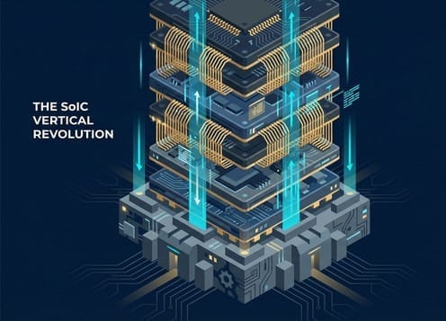
5-3-1 SoIC 3D Packaging Showdown: AMD's 3D Trump Card for a Counterattack Against NVIDIA and Besi's Bumpless Dominance
Analyzing TSMC's SoIC hybrid bonding, achieving atom-level fusion to break traditional 3D packaging bottlenecks. Contrasting NVIDIA's heat-first 2.5D with AMD's 3D stacking performance push; Besi's bumpless tech edge is highlighted. As planar packaging nears limits, 3D structures will be critical...
🧱 The Limits of LEGO Bricks: The "Zig-zag" Labyrinth of Traditional 3D Packaging
To understand cutting-edge 3D packaging, let's first examine how traditional methods work.
In the past, when engineers wanted to stack two chips (e.g., memory and computing cores) one on top of the other, they used "micro-bumps," which we mentioned in 5-2.
You can imagine micro-bumps as the "circular studs on LEGO bricks." When two bricks are to be joined, the groove on the top aligns with the stud on the bottom. Pressing them firmly together, along with high temperatures to melt the solder balls, connects the two chips.
Pain Points of Traditional 3D Packaging
Micro-bumps themselves have volume (typically tens of micrometers in height), creating unavoidable "gaps" between the two chips.
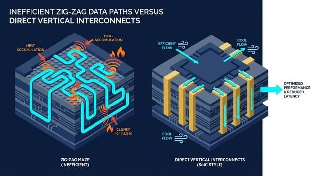
Signals from the bottom layer to the top layer must first travel to the edge, pass through the solder balls, and then route into the upper chip.
This forms a "zig-zag" path, slowing down speed and generating greater electrical resistance and heat at the solder balls.
In the era of AI, which demands ultimate computing power and low latency, this "LEGO-style" stacking method has become a bottleneck hindering performance.
🏗️ The Steel Structure of Skyscrapers: SoIC and the "Bumpless" Revolution
To overcome this physical barrier, TSMC unveiled its ultimate trump card in 3D packaging — SoIC (System on Integrated Chips).
The core technology of SoIC is a cutting-edge technique called "Hybrid Bonding." This technology directly eliminates traditional solder balls and micro-bumps, achieving the "bumpless" state long sought after in the semiconductor industry.
If traditional packaging is like stacking LEGOs, then Hybrid Bonding is like "directly welding the steel structures of two floors together."
Achieving Extreme Planarization: First, CMP (Chemical Mechanical Planarization) equipment is used to polish the surfaces of two wafers to near atomic-level smoothness.
Direct Copper-to-Copper Interconnection: The wafer surfaces are covered with extremely small copper contacts (copper pads). After the machine aligns them with near-zero error, they are directly bonded.
Atomic-Level Fusion: When two extremely smooth copper surfaces are tightly bonded, copper atoms begin to cross boundaries, share electrons, and fuse with each other.
⚡ The Brutal Aesthetics of "Zero Distance"
Once hybrid bonding is successful, two originally independent chips "merge into a naturally integrated superchip" both physically and electrically.
Vertical Through-Connection: Signals no longer navigate a "zig-zag" labyrinth but travel like an elevator, moving directly from the first floor to the second floor via the shortest straight path (virtually 0µm physical distance).
Ten Thousand-fold Density Increase: Because micro-bumps no longer occupy space, the density of copper contacts in the same area can increase by 1,000 to even 10,000 times compared to traditional packaging, achieving an epic liberation of inter-chip bandwidth.
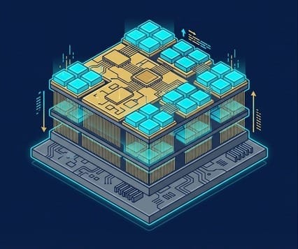
The essence of SoIC is not to "piece together" chips but to "forge" multiple chips into a microscopic skyscraper at an atomic level.
🗺️ NVIDIA's Dominant Philosophy: The "Heat Dissipation Above All" Principle Through Extreme Planarization
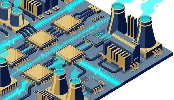
As the undisputed ruler of AI computing power, NVIDIA faces the universe's most demanding challenge: heat.
When a single B200 chip's power consumption exceeds 1000 watts, and future Rubin chips approach 1500 watts, the operating surface temperature of these chips resembles that of a miniature nuclear reactor.
NVIDIA's engineers clearly understand that if two "furnaces" are stacked together (3D packaging), the heat from the bottom chip cannot dissipate, and the entire chip assembly could quickly lose control.
Therefore, NVIDIA adheres to the dominant strategy of CoWoS (2.5D planar packaging): purchasing TSMC's largest "silicon wafer real estate" (interposers) to spread out all GPUs and HBMs on the same plane.
Why planarize? Recall the cutting-edge technology from Hong-Teng (7751) that we mentioned in 5-2-6: only after planarization can a thick metal heat spreader (Lid) be placed over the chips, filled with "pure indium TIM (Thermal Interface Material)" which has extremely high thermal conductivity.
NVIDIA's Logic
“As long as I can suppress the heat, I can infinitely increase clock speeds and computing power. For ultimate heat dissipation, I am willing to spend heavily on the largest silicon wafer real estate and pursue planar expansion.”
🗼 AMD's Surprise Strategy: The "Three-Dimensional Skyscraper" Breaking Boundaries
Facing NVIDIA's strategy of aggressively expanding "planar real estate" through capital and market share, AMD's CEO Lisa Su deeply understood that if AMD played the same flat game, it would always be relegated to second place.
AMD had to launch an asymmetrical three-dimensional surprise attack.
Thus, the industry-shaking MI300 was born.
AMD directly approached TSMC, utilizing the most expensive SoIC (3D Hybrid Bonding). In the MI300's architecture, AMD made an incredibly audacious decision:
Directly "stacking" the CPU chip, responsible for logic control, on top of the GPU chip, responsible for computation.
Or placing SRAM cache memory directly underneath the computing core.
Breaking the Communication Bottleneck (Memory Wall): Utilizing SoIC's copper-to-copper vertical direct connection, CPU and GPU achieve "zero-distance" interconnection, reducing latency and improving power efficiency.
Modular Flexible Building Blocks (Chiplet): Splitting large chips into multiple smaller chiplets to improve yield and cost efficiency, then using 3D space to conserve planar area.
AMD's Logic
“Although my heat dissipation space is limited, through the 'ultra-low transmission power consumption' and 'ultra-high bandwidth' enabled by 3D stacking, I can achieve a performance-to-price ratio that is comparable to, or even surpasses, NVIDIA in specific AI inference and large language model (LLM) tasks.”
🏁 The End Game: When "Planar Real Estate" Becomes Unaffordable
In this showdown between "planar expansion (NVIDIA)" and "vertical stacking (AMD)," NVIDIA's aggressive planar approach remains the market mainstream in terms of market share.
However, if we extend the timeline to the next 3 to 5 years, the scales of victory will irreversibly tip towards 3D skyscrapers.
The reason is very pragmatic: TSMC's silicon wafer real estate is approaching its physical and economic limits.
NVIDIA's CoWoS interposer has expanded from 1 reticle area to 3.3x, 4x, and is even set to challenge 5.5x or more in the future, bringing two devastating problems:
This post is for subscribers only
Sign up now to read the post and get access to the full library of posts for subscribers only.